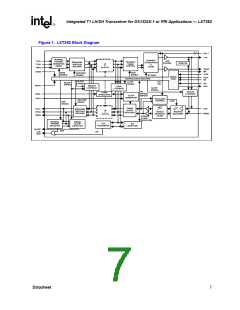
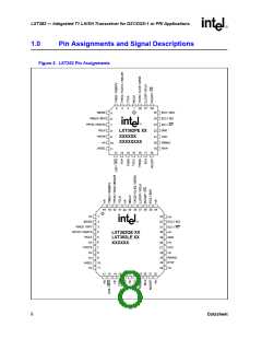
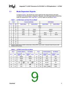
Integrated T1 LH/SH Transceiver for DS1/DSX-1 or PRI Applications — LXT362
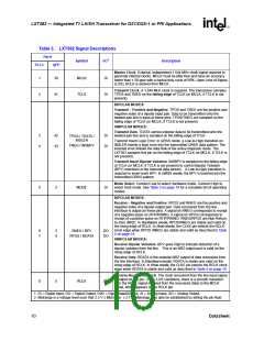
Table 3. LXT362 Signal Descriptions (Continued)
Pin #
PLCC
Symbol
I/O1
Description
QFP
Tristate.
HARDWARE MODES:
Connect TRSTE High to force all output pins to the high impedance state.
TRSTE, in conjunction with the MODE pin, selects the operating modes
listed in Table 5 on page 19.
9
7
TRSTE
DI
HOST MODES:
Connect TRSTE High to force all output pins to the high-impedance state.
Connect this pin Low for normal operation.
HARDWARE MODES:
Jitter Attenuation Select. Selects jitter attenuation location:
Setting JASEL High activates the jitter attenuator in the receive path.
Setting JASEL Low activates the jitter attenuator in the transmit path.
Setting JASEL to Midrange2 disables jitter attenuation.
11
10
JASEL
DI
HOST MODES:
Connect Low in Host mode.
Loss of Signal Indicator. LOS goes High upon receipt of 175 consecutive
spaces and returns Low when the received signal reaches a mark density
of 12.5% (determined by receipt of 16 marks within a sliding window of 128
bits with fewer than 100 consecutive zeros). Note that the transceiver
outputs received marks on RPOS and RNEG even when LOS is High.
12
13
LOS / QPD
DO
AO
QRSS Pattern Detect. In QRSS mode, QPD stays High until the
transceiver detects a QRSS pattern. When a QRSS pattern is detected,
the pin goes Low. Any bit errors cause QPD to go High for half a clock
cycle. This output can be used to trigger an external error counter. Note
that a LOS condition will cause QPD to remain High. See Figure 11.
Transmit Tip and Ring. Differential driver output pair designed to drive a
50 - 200 Ω load. The transformer and line matching resistors should be
selected to give the desired pulse height and return loss performance. See
“Application Information” on page 34.
13
16
15
19
TTIP
TRING
14
15
16
18
TGND
TVCC
-
-
Ground return for the transmit driver power supply TVCC.
+5 VDC Power Supply for the transmit drivers. TVCC must not vary from
VCC by more than ± 0.3 V.
HARDWARE MODES:
Equalization Control 4. Used along with EC3, EC2 and EC1 pins to
specify pulse equalization, line build out and equalizer gain limit settings.
See Table 10 on page 30 for details.
17
18
20
21
EC4
DI
HOST MODES:
Connect Low in Host mode.
Network Loopback Active. Goes High to indicate that Network loopback
(NLOOP) is active. NLOOP is activated by the reception of a 00001 pattern
for five seconds. NLOOP is reset by reception of a 001 pattern for five
seconds, or by activation of Remote loopback (RLOOP).
NLOOP
DO
Receive Tip and Ring. The Alternate Mark Inversion (AMI) signal received
from the line is applied at these pins. A 1:1 transformer is required. Data
and clock recovered from RTIP/RRING are output on the RPOS/RNEG (or
RDATA in Unipolar mode), and RCLK pins.
19
20
24
25
RTIP
AI
-
RRING
+5 VDC Power Supply for all circuits except the transmit drivers. Transmit
drivers are supplied by TVCC.
21
27
VCC
1. DI = Digital Input; DO = Digital Output; DI/O = Digital Input/Output; AI = Analog Input; AO = Analog Output.
2. Midrange is a voltage level such that 2.3 V ≤ Midrange ≤ 2.7 V. Midrange may also be established by letting the pin float.
Datasheet
11

 INTEL [ INTEL ]