XMC4500
XMC4000 Family
Electrical Parameters
3.2
DC Parameters
3.2.1
Input/Output Pins
The digital input stage of the shared analog/digital input pins is identical to the input
stage of the standard digital input/output pins.
Note: These parameters are not subject to production test, but verified by design and/or
characterization.
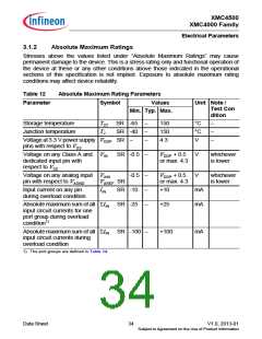
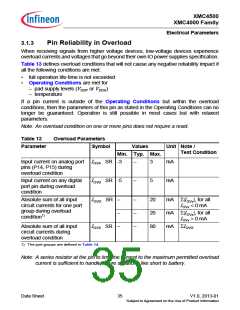
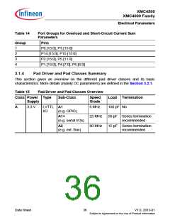
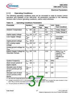
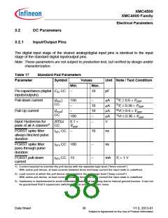
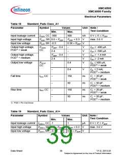
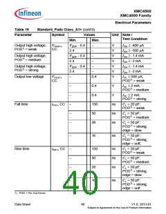
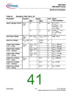
Table 17
Standard Pad Parameters
Parameter
Symbol
Min.
Values
Max.
Unit Note / Test Condition
Pin capacitance (digital CIO CC
−
10
pF
inputs/outputs)
Pull-down current
|IPDL
CC
|
150
−
−
μA
μA
μA
μA
V
1)Vi ≥ 0.6 × VDDP
2)Vi ≤ 0.36 × VDDP
2)Vi ≥ 0.6 × VDDP
1)Vi ≤ 0.36 × VDDP
10
10
−
Pull-Up current
|IPUH
CC
|
−
100
Input Hysteresis for
HYSA
0.1 ×
VDDP
−
pads of all A classes3) CC
PORST spike filter
always blocked pulse
duration
t
t
t
SF1 CC
−
10
−
ns
ns
PORST spike filter
pass-through pulse
duration
SF2 CC 100
SF2 CC 13
PORST pull-down
current
−
mA Vi = 1 V
1) Current required to override the pull device with the opposite logic level (“force current”).
With active pull device, at load currents between force and keep current the input state is undefined.
2) Load current at which the pull device still maintains the valid logic level (“keep current”).
With active pull device, at load currents between force and keep current the input state is undefined.
3) Hysteresis is implemented to avoid metastable states and switching due to internal ground bounce. It can not
be guaranteed that it suppresses switching due to external system noise.
Data Sheet
38
V1.0, 2013-01
Subject to Agreement on the Use of Product Information

 INFINEON [ Infineon ]