XMC4500
XMC4000 Family
Electrical Parameters
3.1.3
Pin Reliability in Overload
When receiving signals from higher voltage devices, low-voltage devices experience
overload currents and voltages that go beyond their own IO power supplies specification.
Table 13 defines overload conditions that will not cause any negative reliability impact if
all the following conditions are met:
•
•
full operation life-time is not exceeded
Operating Conditions are met for
– pad supply levels (VDDP or VDDA
)
– temperature
If a pin current is outside of the Operating Conditions but within the overload
conditions, then the parameters of this pin as stated in the Operating Conditions can no
longer be guaranteed. Operation is still possible in most cases but with relaxed
parameters.
Note: An overload condition on one or more pins does not require a reset.
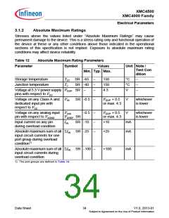
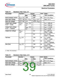
Table 13
Overload Parameters
Symbol
Parameter
Values
Unit Note /
Test Condition
Min. Typ. Max.
Input current on analog port IOVA SR -3
pins (P14, P15) during
–
3
mA
overload condition
Input current on any digital
port pin during overload
condition
IOVD SR -5
–
5
mA
Absolute sum of all input
circuit currents for one port
group during overload
condition1)
IOVG SR –
–
–
–
20
20
80
mA Σ|IOVx|, for all
IOVx < 0 mA
–
mA Σ|IOVx|, for all
IOVx > 0 mA
Absolute sum of all input
circuit currents during
overload condition
IOVS SR
–
mA ΣIOVG
1) The port groups are defined in Table 14.
Note: A series resistor at the pin to limit the current to the maximum permitted overload
current is sufficient to handle failure situations like short to battery.
Data Sheet
35
V1.0, 2013-01
Subject to Agreement on the Use of Product Information

 INFINEON [ Infineon ]