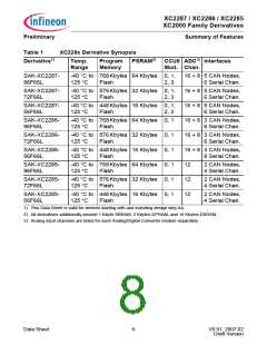
XC2287 / XC2286 / XC2285
XC2000 Family Derivatives
Preliminary
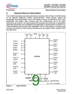
General Device Information
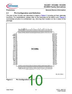
2.1
Pin Configuration and Definition
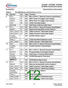
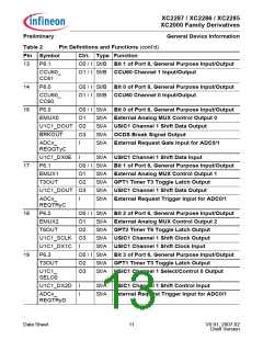
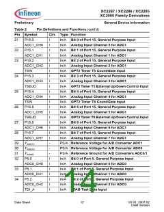
The pins of the XC228x are described in detail in Table 2, including all their alternate
functions. For explanations, please refer to the footnotes at the table’s end. Figure 2
summarizes all pins in a condensed way, showing their location on the 4 sides of the
package.
VSS
VDDPB
VDDPB
1
2
3
4
5
6
7
8
108
107
106
105
104
103
102
101
100
99
P3.7
P0.7
P10.7
P3.6
P10.6
P0.6
P3.5
P10.5
P3.4
P10.4
P3.3
P0.5
TESTM
P7.2
P8.4
TRST
P8.3
P7.0
P7.3
P8.2
P7.1
P7.4
P8.1
9
10
11
12
13
98
97
96
P8.0
VDDIM
14
15
95
94
P10.3
P2.10
P6.0
P6.1
P6.2
16
17
18
19
20
21
22
23
24
25
26
27
28
29
30
31
32
33
34
35
36
93
92
91
90
89
88
87
86
85
84
83
82
81
80
79
78
77
76
75
74
73
P3.2
TRef
VDDI1
P0.4
XC228x
P6.3
VDDPA
P10.2
P3.1
P15.0
P15.1
P15.2
P15.3
P15.4
P15.5
P15.6
P15.7
VAREF1
VAREF0
VAGND
P5.0
P0.3
P10.1
P3.0
P10.0
P0.2
P2.9
P4.7
P2.8
P0.1
P2.7
P4.6
P4.5
P0.0
VDDPB
VSS
P5.1
P5.2
P5.3
VDDPB
MC_XC2X_PIN144
Figure 2
Pin Configuration (top view)
Data Sheet
8
V0.91, 2007-02
Draft Version

 INFINEON [ Infineon ]