XC2287 / XC2286 / XC2285
XC2000 Family Derivatives
Preliminary
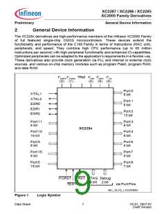
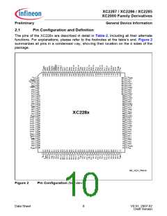
General Device Information
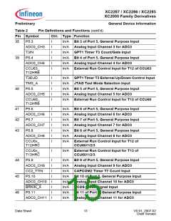
Notes to Pin Definitions
1. Ctrl.: The output signal for a port pin is selected via bitfield PC in the associated
register Px_IOCRy. Output O0 is selected by setting the respective bitfield PC to
1x00B, output O1 is selected by 1x01B, etc.
Output signal OH is controlled by hardware.
2. Type: Indicates the employed pad type (St=standard pad, Sp=special pad,
DP=double pad, In=input pad, PS=power supply) and its power supply domain (A, B,
M, 1).
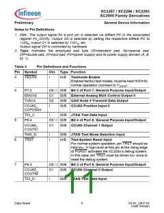
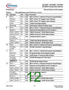
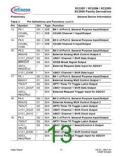
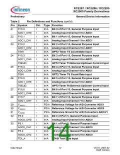
Table 2
Pin Definitions and Functions
Ctrl. Type Function
Pin Symbol
3
TESTM
I
In/B Testmode Enable
Enables factory test modes, must be held HIGH for
normal operation (connect to VDDPB).
4
P7.2
O0 / I St/B Bit 2 of Port 7, General Purpose Input/Output
EMUX0
TxDC4
O1
O2
I
St/B External Analog MUX Control Output 0
St/B CAN Node 4 Transmit Data Output
St/B CCU62 Position Input 0
CCU62_
CCPOS0A
TDI_C
P8.4
I
St/B JTAG Test Data Input
5
6
O0 / I St/B Bit 4 of Port 8, General Purpose Input/Output
CCU60_
COUT61
O1
St/B CCU60 Channel 1 Output
TMS_D
TRST
I
I
St/B JTAG Test Mode Selection Input
In/B Test-System Reset Input
For normal system operation, pin TRST should be
held low. A high level at this pin at the rising edge
of PORST activates the XC228x’s debug system.
In this case, pin TRST must be driven low once to
reset the debug system.
7
P8.3
O0 / I St/B Bit 3 of Port 8, General Purpose Input/Output
CCU60_
COUT60
O1
St/B CCU60 Channel 0 Output
TDI_D
I
St/B JTAG Test Data Input
Data Sheet
9
V0.91, 2007-02
Draft Version

 INFINEON [ Infineon ]