TLE9879QXA40
Electrical Characteristics
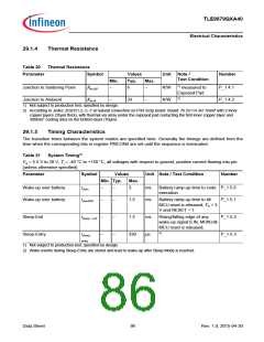
29.1.4
Thermal Resistance
Table 20
Thermal Resistance
Parameter
Symbol
Values
Typ.
6
Unit Note /
Test Condition
Number
Min.
Max.
Junction to Soldering Point
Junction to Ambient
RthJSP
RthJA
–
–
K/W
1) measured to
P_1.4.1
P_1.4.2
Exposed Pad
2)
–
33
–
K/W
1) Not subject to production test, specified by design.
2) According to Jedec JESD51-2,-5,-7 at natural convection on FR4 2s2p board. Board: 76.2x114.3x1.5mm³ with 2 inner
copper layers (35µm thick), with thermal via array under the exposed pad contacting the first inner copper layer and
300mm2 cooling area on the bottom layer (70µm).
29.1.5
Timing Characteristics
The transition times between the system modes are specified here. Generally the timings are defined from the
time when the corresponding bits in register PMCON0 are set until the sequence is terminated.
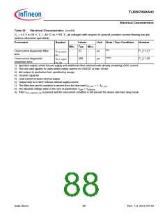
Table 21
System Timing1)
VS = 5.5 V to 28 V, Tj = -40 °C to +150 °C, all voltages with respect to ground, positive current flowing into pin
(unless otherwise specified)
Parameter
Symbol
Values
Min. Typ.
Unit Note / Test Condition
Number
Max.
Wake-up over battery
Wake-up over battery
tstart
–
–
3
ms
ms
Battery ramp-up time to code P_1.5.6
execution
tstartSW
–
–
–
–
1.5
1.5
330
Battery ramp-up time to till
MCU reset is released; VS > 3
V and RESET = 1
P_1.5.1
P_1.5.2
P_1.5.3
Sleep-Exit
tsleep - exit
–
–
ms
µs
Rising/falling edge of any
wake-up signal (LIN, MON) till
MCU reset is released;
2)
Sleep-Entry
tsleep -
entry
1) Not subject to production test, specified by design.
2) Wake events during Sleep-Entry are stored and lead to wake-up after Sleep Mode is reached.
Data Sheet
86
Rev. 1.0, 2015-04-30

 INFINEON [ Infineon ]