TLE9879QXA40
Electrical Characteristics
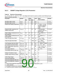
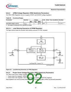
29.2.3
VDDEXT Voltage Regulator (5.0V) Parameters
Table 24
Electrical Characteristics
VS = 5.5 V to 28 V, Tj = -40 °C to +150 °C, all voltages with respect to ground, positive current flowing into pin
(unless otherwise specified)
Parameter
Symbol
Values
Unit Note /
Test Condition
Number
Min.
0
Typ. Max.
Specified output current
Specified output current
IVDDEXT
IVDDEXT
–
–
–
20
40
2.2
mA
mA
µF
–
1)
P_2.3.1
0
P_2.3.21
P_2.3.22
Required decoupling capacitance CVDDEXT1
0.1
3) 2)ESR < 1 Ω; the
specified capacitor
value is a typical
value.
Required buffer capacitance for
stability (load jumps)
CVDDEXT2
1
–
2.2
µF
3)2)the specified
capacitor value is a
typical value.
P_2.3.20
Output voltage including line and VDDEXT
load regulation
4.9
4.8
5.0
5.0
50
–
5.1
5.2
V
V
3) Iload<20mA; VS >
5.5V
P_2.3.3
P_2.3.23
P_2.3.4
P_2.3.14
Output voltage including line and VDDEXT
load regulation
Iload<40mA; VS >
5.5V
3) Iload < 20mA;
3V < VS < 5.0V
Output drop @ Active Mode
Output drop @ Active Mode
VS-VDDEXT
VS-VDDEXT
+300 mV
+400 mV
I
load < 40mA;
3V < VS < 5.0V
2 ... 40mA; C =200nF P_2.3.5
VS = 5.5 ... 28V P_2.3.6
Load regulation @ Active Mode
Line regulation @ Active Mode
VDDEXTLOR -50
VVDDEXTLIR -50
–
–
–
50
50
–
mV
mV
dB
Power supply ripple rejection @ PSSRVDDEXT 50
3) VS = 13.5V; f =0 ... P_2.3.7
Active Mode
1KHz; Vr=2Vpp
Overvoltage detection
VVDDEXTOV 5.18
–
5.4
–
V
VS > 5.5V
3)4)
P_2.3.8
Overvoltage detection filter time tFILT_VDDEXT
–
735
µs
P_2.3.24
OV
3)
3)
Voltage OK detection range
Voltage stable detection range5) ∆VVDDEXTST - 220
VVDDEXTOK
–
3
–
–
V
P_2.3.25
P_2.3.26
+ 220 mV
B
6)
Undervoltage trigger
VVDDEXTUV 2.6
IVDDEXTOC 50
2.8
–
3.0
160
–
V
P_2.3.9
Overcurrent diagnostic
mA
µs
µs
–
3)4)
P_2.3.10
P_2.3.27
P_2.3.28
Overcurrent diagnostic filter time tFILT_VDDCOC
Overcurrent diagnostic shutdown tFILT_VDDCOC
–
–
27
290
3)4)
–
time
_SD
1) This use case requires the reduced utilization of VDDP output current by 20 mA, see P_2.1.22.
2) Ceramic capacitor.
3) Not subject to production test, specified by design.
4) This filter time and its variation is derived from the time base tLP_CLK = 1 / fLP_CLK
.
Data Sheet
90
Rev. 1.0, 2015-04-30

 INFINEON [ Infineon ]