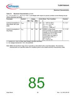
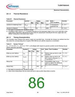
TLE9879QXA40
Electrical Characteristics
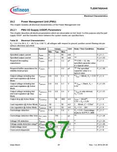
29.2.2
PMU Core Supply (VDDC) Parameters
This chapter describes all electrical parameters which are observable on SoC level. For this purpose only the core-
supply VDDC and the transition times between the system modes are specified here.
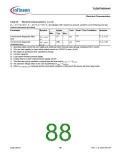
Table 23
Electrical Characteristics
VS = 5.5 V to 28 V, Tj = -40 °C to +150 °C, all voltages with respect to ground, positive current flowing into pin
(unless otherwise specified)
Parameter
Symbol
Values
Min. Typ.
Unit Note /
Test Condition
Number
Max.
Required decoupling capacitance CVDDC1
0.1
–
1
µF
1)2) ESR < 1Ω; the
specified capacitor
value is a typical
value.
P_2.2.1
Required buffer capacitance for
stability (load jumps)
CVDDC2
0.33
–
1
µF
V
2)the specified
capacitor value is a
typical value.
P_2.2.17
P_2.2.2
Output voltage including line
regulation @ Active Mode/Stop
Mode
VDDCOUT 1.44 1.5
1.56
Iload < 40mA
Load Regulation @ Active Mode
Line regulation @ Active Mode
Overvoltage detection
VDDCLOR -50
VDDCLIR -25
VDDCOV
–
–
50
mV
mV
V
2 ... 40mA; C =430nF P_2.2.3
DDP = 2.5 ... 5.5V P_2.2.4
25
V
1.59 1.62
1.68
Overvoltage leads to P_2.2.5
SUPPLY_NMI
1)3)
Overvoltage detection filter time
tFILT_VDDC
–
735
–
µs
P_2.2.18
OV
1)
Voltage OK detection range4)
Voltage stable detection range5)
Undervoltage reset
∆VDDCOK - 280
∆VDDCSTB - 110
–
–
+ 280 mV
+ 110 mV
P_2.2.19
1)
P_2.2.20
VDDVUV
1.136 1.20
1.264
100
–
V
–
P_2.2.6
P_2.2.7
P_2.2.21
Overcurrent diagnostic
IVDDCOC 45
–
mA
µs
–
1)3)
Overcurrent diagnostic filter time tFILT_VDDC
–
–
27
OC
1)3)6)
Overcurrent diagnostic shutdown tFILT_VDDC
290
–
µs
P_2.2.22
time
OC_SD
1) Not subject to production test, specified by design.
2) Ceramic capacitor.
3) This filter time and its variation is derived from the time base tLP_CLK = 1 / fLP_CLK
4) The absolute voltage value is the sum of parameters VDDC + VDDCSTB
5) The absolute voltage value is the sum of parameters VDDC + VDDCOK
6) After tFILT_VDDCOC_SD is passed and the overcurrent condition is still present the device will enter sleep mode.
.
.
.
Data Sheet
89
Rev. 1.0, 2015-04-30

 INFINEON [ Infineon ]