TLE9879QXA40
Electrical Characteristics
29.2
Power Management Unit (PMU)
This chapter includes all electrical characteristics of the Power Management Unit
29.2.1
PMU I/O Supply (VDDP) Parameters
This chapter describes all electrical parameters which are observable on SoC level. For this purpose only the pad-
supply VDDP and the transition times between the system modes are specified here.
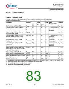
Table 22
Electrical Characteristics
VS = 5.5 V to 28 V, Tj = -40 °C to +150 °C, all voltages with respect to ground, positive current flowing into pin
(unless otherwise specified)
Parameter
Symbol
Values
Unit Note / Test Condition
Number
Min. Typ. Max.
1)
Specified output current
Specified output current
IVDDP
0
–
–
–
50
30
2.2
mA
P_2.1.1
P_2.1.22
P_2.1.2
1)2)
IVDDP
0
mA
Required decoupling
capacitance
CVDDP1
0.47
µF
µF
V
3)4) ESR < 1Ω; the
specified capacitor value
is a typical value.
3)4) The specified
capacitor value is a
typical value.
Required buffer capacitance for CVDDP2
stability (load jumps)
1
–
2.2
5.1
5.1
5.5
400
P_2.1.20
Output voltage including line
and load regulation @ Active
Mode
VDDPOUT 4.9
5.0
5.0
5.0
50
5) Iload < 90mA; VS > 5.5V P_2.1.3
Output voltage including line
and load regulation @ Active
Mode
VDDPOUT 4.9
V
2)5) Iload < 70mA; VS >
5.5V
P_2.1.23
P_2.1.21
P_2.1.4
Output voltage including line
and load regulation @ Stop
Mode
VDDPOUTS 4.5
V
5) Iload is only internal;
VS > 5.5V
TOP
Output drop @ Active Mode
VSVDDPout
–
mV
I
VDDP = 30mA6);
3.5V < VS < 5.0V
2 ... 90mA; C = 570nF
VS = 5.5 ... 28V
Load regulation @ Active Mode VVDDPLOR -50
Line regulation @ Active Mode VVDDPLIR -50
–
–
–
50
50
5.4
mV
mV
V
P_2.1.5
P_2.1.6
Overvoltage detection
VDDPOV
5.14
VS > 5.5V; Overvoltage P_2.1.7
leads to SUPPLY_NMI
3)7)
Overvoltage detection filter time tFILT_VDDP
–
735
–
–
µs
V
P_2.1.24
OV
3)
Voltage OK detection
VDDPOK
–
3
P_2.1.25
3)
Voltage stable detection range8) ∆VDDPSTB - 220
–
+ 220 mV
P_2.1.26
Undervoltage reset
VDDPUV
IVDDPOC
2.5
91
2.6
–
2.7
V
–
–
P_2.1.8
P_2.1.9
Overcurrent diagnostic
220
mA
Data Sheet
87
Rev. 1.0, 2015-04-30

 INFINEON [ Infineon ]