TLE9879QXA40
Electrical Characteristics
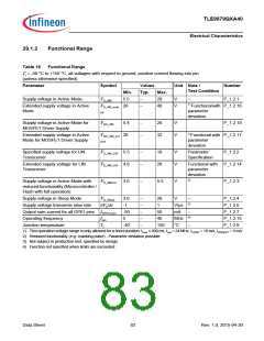
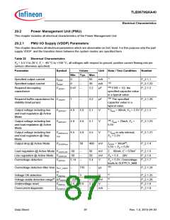
29.1.2
Functional Range
Table 18
Functional Range
Tj = -40 °C to +150 °C, all voltages with respect to ground, positive current flowing into pin
(unless otherwise specified)
Parameter
Symbol
Values
Unit Note /
Test Condition
Number
Min.
Typ.
Max.
28
Supply voltage in Active Mode
VS_AM
5.5
–
–
V
V
–
P_1.2.1
Extended supply voltage in Active
Mode
VS_AM_exte 28
40
1) Functionalwith P_1.2.16
parameter
nd
deviation
Supply voltage in Active Mode for
MOSFET Driver Supply
VSD_AM
5.4
–
–
28
32
V
V
P_1.2.18
Extended supply voltage in Active
Mode for MOSFET Driver Supply
VSD_AM_ext 28
1)Functional with P_1.2.17
parameter
end
deviation
Specified supply voltage for LIN
Transceiver
VS_AM_LIN 5.5
VS_AM_LIN 4.8
–
–
18
28
V
V
Parameter
Specification
P_1.2.2
Extended supply voltage for LIN
Transceiver
Functional with P_1.2.14
parameter
deviation
2)
Supply voltage in Active Mode with
reduced functionality (Microcontroller /
Flash with full operation)
VS_AMmin 3.0
–
5.5
V
P_1.2.3
Supply voltage in Sleep Mode
VS_Sleep
3.0
-1
–
–
–
–
–
28
1
V
–
3)
P_1.2.4
P_1.2.5
P_1.2.7
P_1.2.15
P_1.2.9
Supply voltage transients slew rate
dVS/dt
V/µs
mA
MHz
°C
Output sum current for all GPIO pins IGPIO,sum
-50
5
50
40
150
–
4)
Operating frequency
Junction temperature
fsys
Tj
-40
–
1) This operation voltage range is only allowed for a short duration: tmax ≤ 400 ms, fsys = 24 MHz, IVDDP = 10 mA, IVDDEXT = 5 mA.
2) Reduced functionality (e.g. cranking pulse) - Parameter deviation possible.
3) Not subject to production test, specified by design.
4) Function not specified when limits are exceeded.
Data Sheet
83
Rev. 1.0, 2015-04-30

 INFINEON [ Infineon ]