TLE9879QXA40
Electrical Characteristics
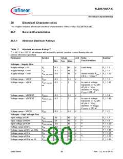
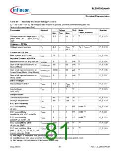
Table 17
Absolute Maximum Ratings1) (cont’d)
Tj = -40 °C to +150 °C, all voltages with respect to ground, positive current flowing into pin
(unless otherwise specified)
Parameter
Symbol
Values
Unit Note /
Test Condition
Number
Min. Typ. Max.
7)
Voltage range at charge pump
pins CP1H, CP1L, CP2H, CP2L,
VCP
VCPx
-0.3
–
48
V
P_1.1.15
Voltages – GPIOs
8)
Voltage on any port pin
Vin
-0.3
–
–
VDDP
+0.3
V
VIN < VDDPmax
P_1.1.16
P_1.1.35
Current at VCP Pin
Max. current at VCP pin
Injection Current at GPIOs
IVCP
-15
-5
–
mA
–
9)
9)
Injection current on any port pin IGPIONM
–
–
5
mA
mA
P_1.1.34
P_1.1.30
Sum of all injected currents in
Normal Mode
IGPIOAM_sum -50
50
9)
9)
Sum of all injected currents in
Power Down Mode (Stop Mode)
IGPIOPD_sum -5000 –
50
5
µA
P_1.1.36
P_1.1.37
Sum of all injected currents in
Sleep Mode
IGPIOSleep_su -5
–
mA
m
Other Voltages
Input voltage VAREF
VAREF
VOAI
-0.3
–
–
VDDP
+0.3
V
V
–
–
P_1.1.17
P_1.1.23
Input voltage
OP1, OP2
-7
7
Temperatures
Junction temperature
Storage temperature
ESD Susceptibility
Tj
-40
-55
–
–
150
150
°C
°C
–
–
P_1.1.18
P_1.1.19
Tstg
ESD susceptibility
all pins
VESD1
-2
–
–
–
–
–
2
kV
kV
kV
V
HBM 10)
HBM 11)
P_1.1.20
P_1.1.21
P_1.1.22
P_1.1.28
P_1.1.43
ESD susceptibility
pins MON, VS, VSD vs.GND
VESD2
-4
4
ESD susceptibility
pins LIN vs. GND_LIN
VESD3
-6
6
HBM 10)
12)
ESD susceptibility CDM
all pins vs. GND
VESD_CDM1
VESD_CDM2
-500
-750
500
750
12)
ESD susceptibility CDM
pins 1, 12, 13, 24, 25, 36, 37, 48
(corner pins) vs. GND
V
1) Not subject to production test, specified by design.
2) Conditions and min. value is derived from application condition for reverse polarity event.
3) Min voltage -28V with external 3.9kΩ series resistor only.
Data Sheet
81
Rev. 1.0, 2015-04-30

 INFINEON [ Infineon ]