TLE9879QXA40
Application Information
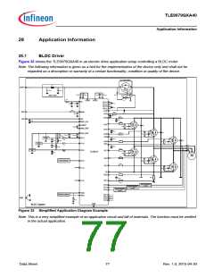
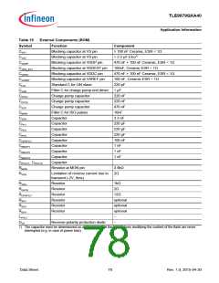
Table 15
Symbol
CVS1
External Components (BOM)
Function
Component
Blocking capacitor at VS pin
Blocking capacitor at VS pin
Blocking capacitor at VDDP pin
Blocking capacitor at VDDEXT pin
Blocking capacitor at VDDC pin
Blocking capacitor at VAREF pin
Standard C for LIN slave
≥ 100 nF Ceramic, ESR < 1Ω
> 2.2 µF Elco1)
CVS2
CVDDP
CVDD_EXT
CVDDC
CVAREF
CLIN
470 nF + 100 nF Ceramic, ESR < 1Ω
100nF, Ceramic ESR < 1Ω
470 nF + 100 nF Ceramic, ESR < 1Ω
100 nF, Ceramic ESR < 1Ω
220 pF
CVSD
Filter C for charge pump end driver 1 µF
CCPS1
CCP2S
CVCP
Charge pump capacitor
Charge pump capacitor
Charge pump capacitor
Filter C for ISO pulses
Capacitor
220 nF
220 nF
470 nF
10nF
CMON
CVDH
3.3 nF
220 µF
220 µF
220 µF
100 nF
1 nF
CPH1
Capacitor
CPH2
Capacitor
CPH3
Capacitor
COPAFILT
CEMCP1
CEMCP2
CEMCP3
Capacitor
Capacitor
Capacitor
1 nF
Capacitor
1 nF
C
PFILT1, CPFILT2
Capacitor
RMON
RVSD
Resistor at MON pin
3.9kΩ
2Ω
Limitation of reverse current due to
transient (-2V, 8ms)
RVDH
RGATE
ROPAFILT
RSH1
Resistor
Resistor
Resistor
Resistor
Resistor
Resistor
1kΩ
2Ω
12Ω
optional
optional
optional
–
RSH2
RSH3
LPFILT
DVS
Reverse-polarity protection diode
–
1) The capacitor must be dimensioned so as to ensure that flash operations modifying the content of the flash are never
interrupted (e.g. in case of power loss).
Data Sheet
78
Rev. 1.0, 2015-04-30

 INFINEON [ Infineon ]