OPTIREG™ SBC TLE9274QXV33
DC/DC regulators
The shunt resistor can be calculated based on VTH,SNS and using Equation (6.1).
VTH ,SNS
(6.1)
RSENSE
=
IOC , peak
Example: for an overcurrent peak detection of 2.1 A, the resistor is typically 0.1 Ω.
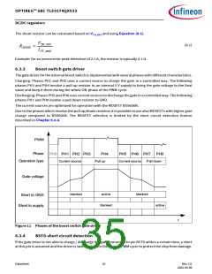
6.3.3
Boost switch gate driver
The gate driver for the external boost switch is implemented with several phases with different characteristics.
Charging: Phases PH1 and PH2 uses a current source to charge the gate in a controlled way. The following
phases PH3 and PH4 involve a pull up resistor to an internal 5 V supply to bring the gate voltage to the final
value and keep it there during the whole ON-phase of the PWM cycle.
Discharging: Phases PH5 and PH6 uses current sources to discharge the gate in a controlled way. The following
phases PH7 and PH0 involve a pull down resistor to GND.
The current sources are optimized for operation with the MOSFET BSS606N.
Due to the phases which involve the pull up/down resistors it is possible to use also MOSFETs with higher gate
charge compared to BSS606N. The MOSFET selection is limited by the short circuit detection feature
described in Chapter 6.3.4.
PWM
Phase
PH0 PH1 PH2 PH3
Current source
PH4
PH5 PH6 PH7 PH0
Operation type
Pull up
Current source
Pull down
Gate voltage
blanked
active
blanked
Short to GND
blanked
active
Short to supply
t
Figure 11 Phases of the boost switch gate driver
6.3.4
BSTG short circuit detection
If the gate driver is not able to charge / discharge the gate connected to pin BSTG within a certain time, a short
at this pin is assumed and the driver is switched off for the current PWM cycle to protect the chip from damage.
Datasheet
35
Rev.2.0
2022-05-06

 INFINEON [ Infineon ]