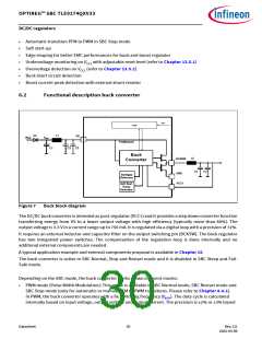
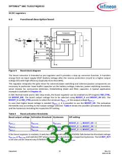
OPTIREG™ SBC TLE9274QXV33
DC/DC regulators
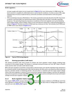
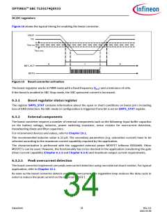
Figure 10 shows the typical timing for enabling the boost converter.
VSUP
VS
VBST,THx
VBST,HYSx
0
1
0
BST_ACT
BSTG
Figure 10 Boost converter activation
The boost regulator works in PWM mode with a fixed frequency (fBST) and a tolerance of ±5%.
If the boost is enabled in SBC Stop mode, the SBC quiescent current is increased.
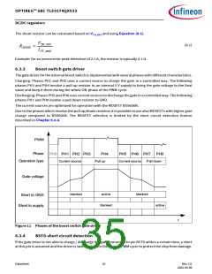
6.3.1
Boost regulator status register
The register SMPS_STAT contains information about the open or short conditions on boost pin’s including
loss of GND detection. No SBC mode or configuration is triggered if one bit is set on SMPS_STAT register.
6.3.2
External components
The boost converter requires a number of external components such as the following: input buffer capacitor
on the battery voltage, inductor, power switching transistor, sense resistor for overcurrent detection,
freewheeling diode and filter capacitors.
For recommend devices and values, refer to Chapter 15.1.
The recommended inductor value is 22 µH. The secondary parameters (e.g. saturation current) have to be
selected according to the maximum current capability required by the application.
The characterization is performed with the suggested external power MOSFET Infineon BSS606N. Other
MOSFETs can be used. However, the functionality has to be checked in the application considering the gate
driver current capability (Chapter 6.3.3 and Chapter 6.3.4) and maximum output current requirements.
6.3.2.1 Peak overcurrent detection
The boost converter implement one peak overcurrent detection using one external shunt resistor. For typical
application, refer to Chapter 15.1.
As soon as the boost converter detects one peak overcurrent, the regulation loop reduces the duty cycle in
order to reduce the peak current on the external MOSFET.
Datasheet
34
Rev.2.0
2022-05-06

 INFINEON [ Infineon ]