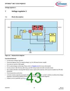
OPTIREG™ SBC TLE9274QXV33
DC/DC regulators
6.5
Electrical characteristics
Table 10 Electrical characteristics
Tj = -40°C to +150°C; VS = 5.5 V to 28 V; all voltages with respect to ground, positive current flowing into pin
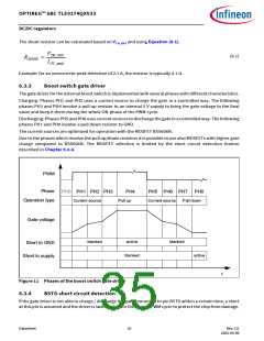
(unless otherwise specified)
Parameter
Symbol
Values
Unit Note or Test Condition Number
Min. Typ. Max.
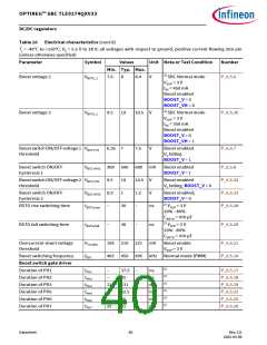
Buck regulator
Output voltage SBC Normal
mode
VCC1,out1 3.23 3.3 3.36
VCC1,out2 3.23 3.3 3.36
V
V
Normal mode (PWM)
1 mA < IVCC1 < 750 mA
6.3 V < VS < 28 V
1)Normal mode (PWM)
IVCC1 = 400 mA
VS = 4 V
P_6.5.12
P_6.5.24
Output voltage SBC Normal
mode
Boost disabled
Output voltage SBC Stop
mode
VCC1,out3 3.16 3.3 3.43
VCC1,out4 3.18 3.3 3.39
V
V
Stop mode (PFM)
1 mA < IVCC1 < IPFM-PWM,TH
6.3 V < VS < 18 V
P_6.5.13
P_6.5.41
Output voltage SBC Stop
mode
Stop mode (PFM)
1 mA < IVCC1 < 50 mA
6.3 V < VS < 18 V
Power Stage on-resistance
High-Side
RDSON1,HS
RDSON1,LS
–
–
–
–
1.3
1.3
Ω
Ω
VS = 6.5 V
IVS= 100 mA
P_6.5.3
Power Stage on-resistance
Low-Side
IBCKSW= 100 mA
P_6.5.20
Buck switching frequency
fBCK
405 450 495 kHz Normal mode (PWM)
P_6.5.5
Threshold automatic
transition PFM to PWM
IPFM-
PWM,TH
80
110 150 mA 2) Stop mode
P_6.5.14
6.3 V < VS < 18 V
Transition time from PWM to tlag
PFM
–
1
–
–
ms
µs
A
2) PWM_TLAG=1
(on HW_CTRL)
2) PWM_TLAG=0
(on HW_CTRL)
P_6.5.15
P_6.5.16
P_6.5.4
Transition time from PWM to tlag
PFM
–
100
Peak current limit of internal IBCK_LIM
high-side switch
0.85 1.05 1.2
6.32 6.65 6.88
VS = 13.5 V
Boost regulator
Boost voltage 1
VBST1_1
V
3) SBC Normal mode
P_6.5.11
VSUP = 3 V
IVS = 550 mA
Boost enabled
BOOST_V = 1
BOOST_VH = X
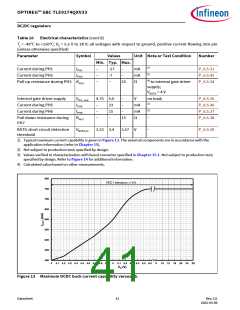
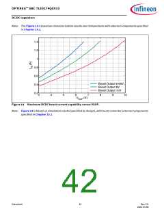
Datasheet
39
Rev.2.0
2022-05-06

 INFINEON [ Infineon ]