OPTIREG™ SBC TLE9274QXV33
DC/DC regulators
6.3
Functional description boost
Comparator
VSENSE
VS
D1
L1
D2
Vbat
VSUP
SPI
Boost
Converter
C1
C2
C3
BSTD
BSTG
T1
SNSP
SNSN
Rsense
VS
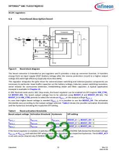
Figure 9
Boost block diagram
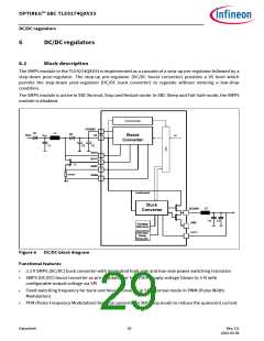
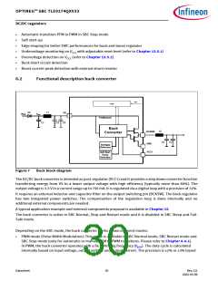
The boost converter is intended as pre-regulator and it provides a step up converter function. It transfers
energy from an input supply VSUP (battery voltage after the reverse protection circuit) to a higher output
voltage (VS) with high efficiency (typically more than 80%).
The regulator integrates the gate driver for external power switching and external passive components are
necessary in particular: input buffer capacitor on the battery voltage, inductor, power switching transistor,
sense resistor for overcurrent detection, freewheeling diode and filter capacitor. A typical application
example is available in Chapter 15.
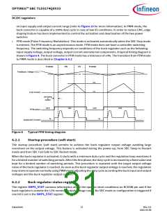
In SBC Normal mode and in SBC Stop mode, the boost regulator can be enabled via SPI (register HW_CTRL,
bit BOOST_EN). The boost output voltage has to be selected using BOOST_V and BOOST_VH bits. The
BOOST_V on HW_CTRL permits to select the minimum VBST1_1 or the output voltage VBST2_1
.
In case that higher boost voltage is needed (VBST3_1), it is possible to use the BOOST_VH. The activation
thresholds vary according to the output voltage selected. Table 9 shows the possible activation thresholds
and the hysteresis including the respective SPI setting.
Table 9
Boost activation thresholds
Boost output voltage Activation threshold Hysteresis
SPI setting
VBST1_1
VBST2_1
VBST3_1
VBST,TH1
VBST,TH2
VBST,TH2
VBST,HYS1
VBST,HYS2
VBST,HYS2
BOOST_V = 1, BOOST_VH = X
BOOST_V = 0, BOOST_VH = 0
BOOST_V = 0, BOOST_VH = 1
If the boost regulator is enabled, it switches ON automatically when VSENSE falls below the threshold voltage
BST,TH1 or VBST,TH2 and switches OFF when crossing the threshold plus respective hysteresis. The bit BST_ACT
is set and can be cleared only if VSENSE is above the VBST,TH1 or VBST,TH2
V
.
Datasheet
33
Rev.2.0
2022-05-06

 INFINEON [ Infineon ]