OPTIREG™ SBC TLE9274QXV33
System features
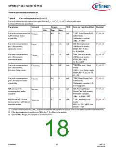
No watchdog trigger during the long open window, will cause a watchdog failure and the device will enter in
SBC Restart mode as shown in Table 6 and one reset event is generated.
In case of 3 consecutive reset events due to WD failures, it is possible not to generate additional reset by
setting the MAX_3_RST on WD_CTRL and the SBC will remain in SBC Normal or Stop mode (SBC Restart mode
not entered anymore). If the MAX_3_RST is set to 0, one reset event is generated for each missing watchdog
trigger.
Wake-up events are ignored during SBC Init mode and will therefore be lost.
Notes
1. Any SPI command will bring the SBC to SBC Normal mode even if it is an illegal SPI command
(see Chapter 14.2).
2. For a safe start-up, it is recommended to use the first SPI commands to trigger and to configure the
watchdog.
3. At power up no VCC1_UV will be issued nor will the FOx be triggered as long as VCC1 is below VRT1,r threshold
and below the VS threshold for VS under voltage time out VS,UV_TO. The RO pin will be kept low as long as VCC1
is below the selected VRT1,r threshold. When VCC1 is above the VRT1,r threshold, the RO is released after tRD1
(Reset delay time).
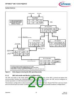
5.1.2
SBC Normal mode
The SBC Normal mode is the standard operating mode for the SBC. All configurations have to be done in
SBC Normal mode before entering a low-power mode. A wake-up event on CAN LIN1, LIN2, LIN3, LIN4 and WK
will create an interrupt on pin INT however, no changes of SBC mode will occur. The configuration options are
listed below:
•
•
VCC1 is active (buck regulator in PWM mode)
Boost regulator can be configured and enabled or disabled. The module will start to work as soon as the
VS value is dropping below the selected threshold. For additional information, refer to Chapter 6.3
•
•
VCC2 can be switched ON or OFF (default off)
CAN is configurable (OFF coming from SBC Init mode; OFF or wake capable coming from SBC Restart mode,
see also Chapter 5.1.5)
•
LIN is configurable (OFF coming from SBC Init mode; OFF or wake capable coming from SBC Restart mode,
see also Chapter 5.1.5)
•
•
•
•
Wake pin shows the input level and can be selected to be wake capable
Cyclic wake can be configured with timer1
Watchdog is configurable
FO1 and FO3 are OFF and FSI is active by default. FSI can be configured to be fail-safe output (see also
Chapter 12.2). Coming from SBC Restart mode, the FOx can be active or inactive (see also Chapter 12.1)
In SBC Normal mode, there is the possibility of testing the FO outputs, i.e. to verify if setting the FOx pins to
low will create the intended behavior within the system. The FO outputs can be enabled and then disabled
again by the microcontroller by setting the FO_ON SPI bit. The feature is only intended for testing purposes.
5.1.3
SBC Stop mode
The SBC Stop mode is the first level technique to reduce the overall current consumption. In this mode
VCC1 regulator is still active and supplying the microcontroller, which can enter into a power down mode.
Datasheet
22
Rev.2.0
2022-05-06

 INFINEON [ Infineon ]