OPTIREG™ SBC TLE9274QXV33
System features
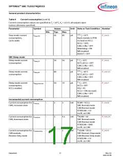
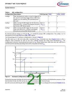
Table 6
SBC configuration
Configuration Description
FO3/Test pin TEST
CFG2_ STATE
Config 0
SBC Development mode: no reset is triggered 0
1
X
in case of a watchdog trigger failure. After the
power-up, one arbitrary SPI command must
be sent
Config 1
Config 3
After missing the WD trigger for the first time, Open or
the state of VCC1 remains unchanged, FOx pins > VTEST,H
are active, SBC Restart mode
0
0
1
0
After missing the WD trigger for the second
time, the state of VCC1 remains unchanged,
FOx pins are active, SBC Restart mode
Open or
> VTEST,H
An external pull-up resistor on CFG pin (RCFG) is needed for proper SBC configuration. The config 1 or 3 is
selectable via SPI using CFG2 bit on HW_CTRL register.
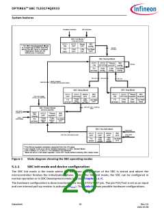
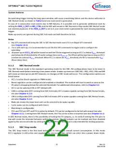
The timing diagram for hardware configuration is shown in Figure 4.
The SBC starts up in SBC Init mode after crossing the VPOR,r threshold (see also Chapter 13.3) or after a
software reset command. As soon as the VCC1 voltage reaches the rising reset threshold VRT1,r, the
configuration selection monitoring period starts for tRD1 (Reset delay time). After this time, the reset pin is
released and the window watchdog starts with a long open window tLW
.
VS
VPOR,r
t
t
VCC1
VRT1,r
RO
t
tRD1
Configuration selection monitoring period
Figure 4
Hardware configuration selection timing diagram
During the long open window, the microcontroller needs to finish its startup and initialization sequence. From
this transition mode, the SBC can be set, via SPI command, to SBC Normal mode.
Any SPI command will bring the SBC to SBC Normal mode even if it is an illegal SPI command (Chapter 14.2).
Datasheet
21
Rev.2.0
2022-05-06

 INFINEON [ Infineon ]