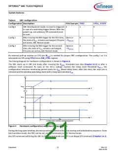
OPTIREG™ SBC TLE9274QXV33
System features
•
•
•
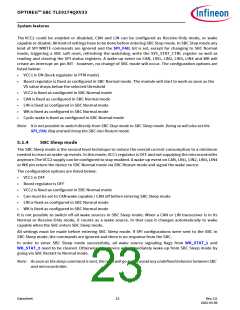
RO is pulled low during SBC Restart mode
SPI communication is ignored by the SBC, i.e. it is not interpreted
SBC Restart mode is signalled in the SPI register DEV_STAT by DEV_STAT bits
Note: The VCC1 overvoltage reset is by default disabled. To enable it, the VCC1_OV_ RST has to be set. For
additional information, refer to Chapter 13.5.2.
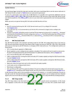
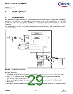
5.1.6
SBC Fail-Safe mode
The purpose of this mode is to bring the system in a safe status after a failure condition by turning off the
VCC1 regulator and the RO will be LOW. After a wake-up event, the system can restart.
The Fail-Safe mode is automatically reached in case of following events:
•
•
Overtemperature (TSD2) (see also Chapter 13.8)
VCC1 is shorted to GND (see also Chapter 13.5.3)
In this case, the default wake sources are activated and the voltage regulators are switched OFF.
The mode will be maintained for at least typical 1s (tTSD2) for a TSD2 event and typical 100 ms (tFS,min) for the
other failure events to avoid any fast toggling behavior. All wake sources will be disabled during this time but
wake-up events will be stored. Stored wake-up events and wake-up events after this minimum waiting time
will lead to SBC Restart mode. Leaving the SBC Fail-Safe mode will not result in deactivation of the FOx pins.
The following functions are influenced during SBC Fail-Safe mode:
•
•
•
•
•
•
•
•
•
FO outputs are activated (see also Chapter 12)
VCC1 is OFF
Boost regulator is OFF
VCC2 is OFF
CAN is wake capable
LINx are wake capable
WK is wake capable
Cyclic wake is disabled, static sense is active with default filter time
SPI communication is disabled because VCC1 is OFF
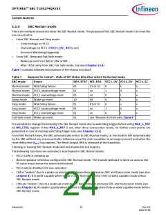
Table 8
Mode
Reasons for fail-safe - state of SPI status bits after return to Normal mode
Config Event
1, 3 TSD2
1, 3, 4 VCC1 short to GND
DEV_STAT TSD2
WD_FAIL
VCC1_UV
VCC1_SC
Normal
Normal
01
01
01
01
1
x
1
x
xx
xx
xx
xx
x
1
x
1
0
1
0
1
Stop mode 1, 3
Stop mode 1, 3
TSD2
VCC1 short to GND
Datasheet
25
Rev.2.0
2022-05-06

 INFINEON [ Infineon ]