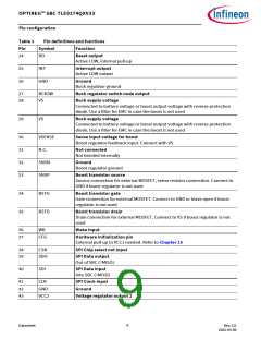
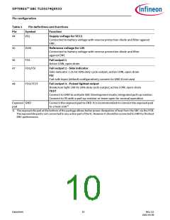
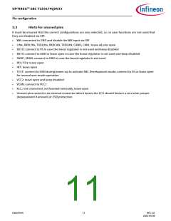
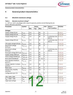
OPTIREG™ SBC TLE9274QXV33
General product characteristics
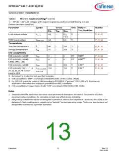
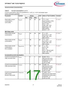
Table 2
Absolute maximum ratings1) (cont’d)
Tj = -40°C to +150°C; all voltages with respect to ground, positive current flowing into pin
(unless otherwise specified)
Parameter
Symbol
Values
Typ.
–
Unit Note or
Test Condition
Number
Min.
Max.
Logic output voltage
VO, max
-0.3
VCC1
+ 0.3
V
–
P_4.1.27
P_4.1.11
VCAN Input voltage
Temperatures
VVCAN, max
-0.3
–
5.5
V
–
Junction temperature
Storage temperature
ESD susceptibility
ESD resistivity to GND
Tj
-40
-55
–
–
150
150
°C
°C
–
–
P_4.1.13
P_4.1.14
Tstg
VESD
VESD
-2
-8
–
–
2
8
kV
kV
HBM2)
HBM3)2)
P_4.1.15
P_4.1.16
ESD resistivity to GND,
CANH, CANL, LINx
ESD resistivity to GND
VESD
-500
–
–
500
750
V
V
CDM4)
CDM4)
P_4.1.17
P_4.1.18
ESD resistivity pin 1, 12, 13, VESD1,12,13,24, -750
24, 25, 36, 37, 48 (corner
25,36,37,48
pins) to GND
1) Not subject to production test, specified by design.
2) ESD susceptibility, “HBM” according to ANSI/ESDA/JEDEC JS-001 (1.5 kΩ, 100 pF).
3) For ESD GUN resistivity, tested at 6 kV (according to IEC61000-4-2 “gun test” (330 Ω, 150 pF)), it is shown in
application information and test report, provided from IBEE, is available.
4) ESD susceptibility, Charged Device Model “CDM” according to ANSI/ESDA/JEDEC JS-002.
Notes
1. Stresses above the ones listed here may cause permanent damage to the device. Exposure to absolute
maximum rating conditions for extended periods may affect device reliability.
2. Integrated protection functions are designed to prevent IC destruction under fault conditions described in the
datasheet. Fault conditions are considered as “outside” normal operating range. Protection functions are not
designed for continuous repetitive operation.
Datasheet
13
Rev.2.0
2022-05-06

 INFINEON [ Infineon ]