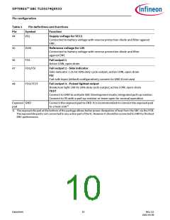
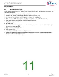
OPTIREG™ SBC TLE9274QXV33
General product characteristics
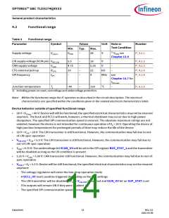
4.2
Functional range
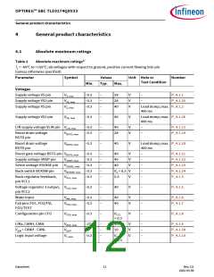
Table 3
Functional range
Parameter
Symbol
Values
Typ.
–
Unit Note or
Test Condition
Number
Min.
Max.
1)
Supply voltage
VS,func
VPOR
28
V
V
see
P_4.2.1
POR
Chapter 13.9
LIN supply voltage (VLIN pin) VREF,LIN
5.5
4.75
10
–
–
–
–
18
5.25
22
4
V
P_4.2.2
P_4.2.3
P_4.2.6
P_4.2.4
CAN supply voltage
CFG external pull-up
SPI frequency
VCAN
RCFG
fSPI
V
–
–
kΩ
–
MHz see
Chapter 14.7 for
fSPI,max
Junction temperature
Tj
-40
–
150
°C
–
P_4.2.5
1) Including power-on reset, overvoltage and undervoltage protection.
Note: Within the functional range the IC operates as described in the circuit description. The electrical
characteristics are specified within the conditions given in the related electrical characteristics table.
Device behavior outside of specified functional range
•
28 V < VS,func < 40 V: Device will still be functional; the specified electrical characteristics may not be ensured
anymore. The buck and VCC2 will work, however, a thermal shutdown may occur due to high power
dissipation. The specified SPI communication speed is ensured. The absolute maximum ratings are not
violated, however the device is not intended for continuous operation of VS > 28 V. Operating the device at
high junction temperatures for prolonged periods of time may reduce the life of the device
•
•
•
•
•
18 V < VLIN < 28 V: The LIN transceiver is still functional. However, the communication may fail due to out-
of-LIN-spec operation
V
LIN,UVD < VLIN < 5.5 V: The LIN transceiver is still functional. However, the communication may fail due to
out-of-LIN-spec operation
CAN < 4.75 V: The undervoltage bit VCAN_UV will be set in the SPI register BUS_STAT_1 and the transmitter
V
will be disabled as long as the UV condition is present
5.25 V < VCAN < 5.50 V: CAN transceiver still functional. However, the communication may fail due to out-of-
spec operation
VPOR,f < VS < 5.5 V: Device will be still functional; the specified electrical characteristics may not be ensured
anymore:
–
–
–
–
–
The voltage regulators will enter the low-drop operation mode
A VCC1_UV reset could be triggered depending on the Vrtx settings
The LIN transmitter will be disabled if VLIN < VLIN,UVD is reached and VLIN_UV bit on SUP_STAT is set
FOx outputs will remain ON if they were enabled
The specified SPI communication speed is ensured
Datasheet
14
Rev.2.0
2022-05-06

 INFINEON [ Infineon ]