OPTIREG™ SBC TLE9274QXV33
Pin configuration
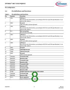
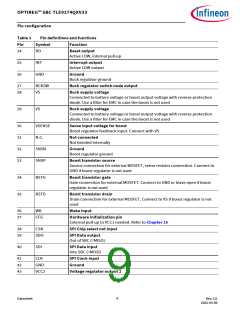
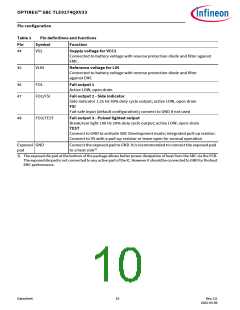
Table 1
Pin
Pin definitions and functions
Symbol
Function
24
RO
Reset output
Active LOW, internal pull-up
25
26
INT
GND
Interrupt output
Active LOW output
Ground
Buck regulator ground
27
28
BCKSW
VS
Buck regulator switch node output
Buck supply voltage
Connected to battery voltage or boost output voltage with reverse protection
diode. Use a filter for EMC in case the boost is not used
29
VS
Buck supply voltage
Connected to battery voltage or boost output voltage with reverse protection
diode. Use a filter for EMC in case the boost is not used
30
31
32
33
VSENSE
N.C.
Sense input voltage for boost
Boost regulator feedback input. Connect with VS
Not connected
Not bonded internally
SNSN
SNSP
Ground
Boost regulator ground
Boost transistor source
Source connection for external MOSFET, sense resistor connection. Connect to
GND if boost regulator is not used
34
35
BSTG
BSTD
Boost transistor gate
Gate connection for external MOSFET. Connect to GND or leave open if boost
regulator is not used
Boost transistor drain
Drain connection for external MOSFET. Connect to VS if boost regulator is not
used
36
37
WK
Wake input
CFG
Hardware initialization pin
External pull-up to VCC1 needed. Refer to Chapter 15
38
39
CSN
SDO
SPI Chip select not input
SPI Data output
Out of SBC (=MISO)
40
SDI
SPI Data input
Into SBC (=MOSI)
41
42
43
CLK
SPI Clock input
Ground
GND
VCC2
Voltage regulator output 2
Datasheet
9
Rev.2.0
2022-05-06

 INFINEON [ Infineon ]