OPTIREG™ SBC TLE9274QXV33
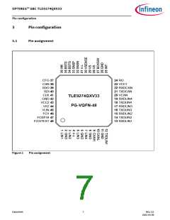
Pin configuration
Table 1
Pin
Pin definitions and functions
Symbol
Function
44
VS2
Supply voltage for VCC2
Connected to battery voltage with reverse protection diode and filter against
EMC.
45
VLIN
Reference voltage for LIN
Connected to battery voltage with reverse protection diode and filter
against EMC
46
47
FO1
Fail output 1
Active LOW, open drain
FO2/FSI
Fail output 2 - Side indicator
Side indicator 1.25 Hz 50% duty cycle output; active LOW, open drain
FSI
Fail-safe input (default configuration); connect to GND if not used
48
FO3/TEST
Fail output 3 - Pulsed lighted output
Break/rear light 100 Hz 20% duty cycle output; active LOW, open-drain
TEST
Connect to GND to activate SBC Development mode; integrated pull-up resistor.
Connect to VS with a pull-up resistor or leave open for normal operation
Exposed GND
pad
Connect the exposed pad to GND. It is recommended to connect the exposed pad
to a heat sink1)
1) The exposed die pad at the bottom of the package allows better power dissipation of heat from the SBC via the PCB.
The exposed die pad is not connected to any active part of the IC. However it should be connected to GND for the best
EMC performance.
Datasheet
10
Rev.2.0
2022-05-06

 INFINEON [ Infineon ]