TLE9263QX
General Product Characteristics
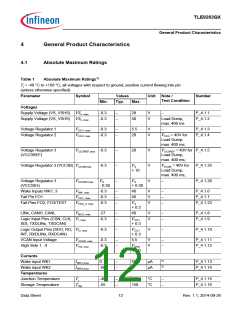
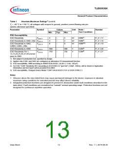
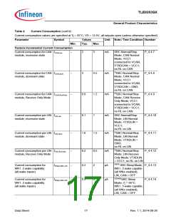
Table 1
Absolute Maximum Ratings1) (cont’d)
Tj = -40 °C to +150 °C; all voltages with respect to ground, positive current flowing into pin
(unless otherwise specified)
Parameter
Symbol
Values
Typ.
Unit Note /
Test Condition
Number
Min.
Max.
ESD Susceptibility
ESD Resistivity
VESD,11
-2
-2
-8
–
–
–
2
2
8
kV
kV
kV
HBM3)
HBM3)
HBM4)3)
P_4.1.17
P_4.1.18
P_4.1.19
ESD Resistivity to GND, HSx VESD,12
ESD Resistivity to GND,
CANH, CANL, LINx
VESD,13
ESD Resistivity to GND
VESD,21
VESD,22
-500
-750
–
–
500
750
V
V
CDM5)
CDM5)
P_4.1.20
P_4.1.21
ESD Resistivity Pin 1,
12,13,24,25,36,37,48 (corner
pins) to GND
1) Not subject to production test, specified by design.
2) Applies only if WK1 and WK2 are configured as alternative HV-measurement function
3) ESD susceptibility, HBM according to ANSI/ESDA/JEDEC JS-001 (1.5 kꢀ, 100 pF)
4) For ESD “GUN” Resistivity 6KV (according to IEC61000-4-2 “gun test” (150pF, 330ꢀ)), will be shown in Application
Information and test report will be provided from IBEE
5) ESD susceptibility, Charged Device Model “CDM” EIA/JESD22-C101 or ESDA STM5.3.1
Notes
1. Stresses above the ones listed here may cause permanent damage to the device. Exposure to absolute
maximum rating conditions for extended periods may affect device reliability.
2. Integrated protection functions are designed to prevent IC destruction under fault conditions described in the
data sheet. Fault conditions are considered as “outside” normal operating range. Protection functions are not
designed for continuous repetitive operation.
Data Sheet
13
Rev. 1.1, 2014-09-26

 INFINEON [ Infineon ]