TLE9263QX
Pin Configuration
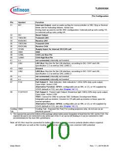
Pin
Symbol
Function
31
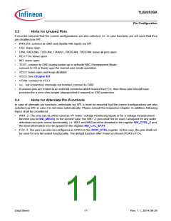
INT
Interrupt Output; used as wake-up flag for microcontroller in SBC Stop or Normal
Mode and for indicating failures. Active low.
During start-up used to set the SBC configuration. External pull-up sets config 1/3,
no external pull-up sets config 2/4.
32
33
34
35
36
37
38
39
40
41
42
RO
Reset Output
TXDLIN1
RXDLIN1
TXDCAN
RXDCAN
VCAN
GND
Transmit LIN1
Receive LIN1
Transmit CAN
Receive CAN
Supply Input; for internal HS-CAN cell
GND
CANL
CAN Low Bus Pin
CAN High Bus Pin
not connected; internally not bonded.
CANH
n.c.
LIN1
LIN1 Bus; Bus line for the LIN interface, according to ISO. 9141 and LIN
specification 2.2 as well as SAE J2602-2.
43
44
GND
LIN2
Ground
LIN2 Bus; Bus line for the LIN interface, according to ISO. 9141 and LIN
specification 2.2 as well as SAE J2602-2.
45
46
47
n.c.
n.c.
FO2
not connected; internally not bonded.
not connected; internally not bonded.
Fail Output 2 - Side Indicator; Side indicators 1.25Hz 50% duty cycle output;
Open drain. Active LOW.
Alternative Function: GPIO1; configurable pin as WK, or LS, or HS supplied by
VSHS (default is FO2, see also Chapter 14.1.1)
48
FO3/TEST
Fail Output 3 - Pulsed Light Output; Break/rear light 100Hz 20% duty cycle output;
Open drain. Active LOW
TEST; Connect to GND to activate SBC Software Development Mode;
Integrated pull-up resistor. Connect to VS with pull-up resistor or leave open for
normal operation.
Alternative Function: GPIO2; configurable pin as WK, or LS, or HS supplied by
VSHS (default is FO3, see also Chapter 14.1.1)
Cooling GND
Tab
Cooling Tab - Exposed Die Pad; For cooling purposes only, do not use as an
electrical ground.1)
1) The exposed die pad at the bottom of the package allows better power dissipation of heat from the SBC via the PCB. The
exposed die pad is not connected to any active part of the IC an can be left floating or it can be connected to GND
(recommended) for the best EMC performance.
Note:all VS Pins must be connected to battery potential or insert a reverse polarity diodes where required;
all GND pins as well as the Cooling Tab must be connected to one common GND potential;
Data Sheet
10
Rev. 1.1, 2014-09-26

 INFINEON [ Infineon ]