TLE9263QX
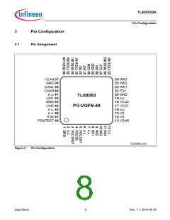
Pin Configuration
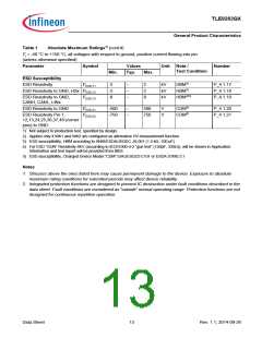
3.2
Pin Definitions and Functions
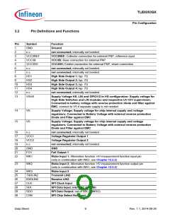
Pin
1
Symbol
Function
GND
n.c.
Ground
2
not connected; internally not bonded.
3
VCC3REF
VCC3B
VCC3SH
n.c.
VCC3REF; Collector connection for external PNP, reference input
VCC3B; Base connection for external PNP
VCC3SH; Emitter connection for external PNP, shunt connection
not connected; internally not bonded.
not connected; internally not bonded.
High Side Output 1; typ. 7Ω
4
5
6
7
n.c.
8
HS1
9
HS2
High Side Output 2; typ. 7Ω
10
11
12
13
HS3
High Side Output 3; typ. 7Ω
HS4
High Side Output 4; typ. 7Ω
n.c
not connected; internally not bonded.
VSHS
Supply Voltage HS, LIN and GPIO1/2 in HS configuration; Supply voltage for
High-Side Switches and LIN modules and respective UV-/OV supervision;
Connected to battery voltage with reverse protection diode and filter against
EMC; connect to VS if separate supply is not needed
14
15
VS
VS
Supply Voltage; Supply voltage for chip internal supply and voltage
regulators; Connected to Battery Voltage with external reverse protection
Diode and Filter against EMC
Supply Voltage; Supply voltage for chip internal supply and voltage
regulators; Connected to Battery Voltage with external reverse protection
Diode and Filter against EMC
16
17
18
19
20
21
22
n.c.
not connected; internally not bonded.
Voltage Regulator Output 1
Voltage Regulator Output 2
not connected; internally not bonded.
GND
VCC1
VCC2
n.c.
GND
FO1
WK1
Fail Output 1
Wake Input 1; Alternative function: HV-measurement function input pin
(only in combination with WK2, see Chapter 12.2.2)
23
WK2
Wake Input 2; Alternative function: HV-measurement function output pin
(only in combination with WK1, see Chapter 12.2.2)
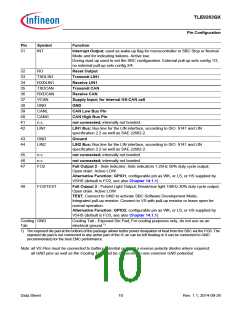
24
25
26
27
28
29
30
WK3
Wake Input 3
TXDLIN2
RXDLIN2
CLK
Transmit LIN2
Receive LIN2
SPI Clock Input
SDI
SPI Data Input; into SBC (=MOSI)
SPI Data Output; out of SBC (=MISO)
SPI Chip Select Not Input
SDO
CSN
Data Sheet
9
Rev. 1.1, 2014-09-26

 INFINEON [ Infineon ]