TLE9263QX
General Product Characteristics
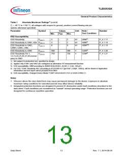
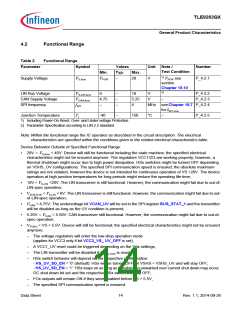
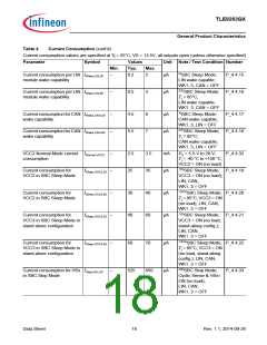
4.2
Functional Range
Table 2
Functional Range
Parameter
Symbol
Values
Typ.
–
Unit Note /
Number
Test Condition
Min.
Max.
Supply Voltage
VS,func
VPOR
28
V
1) VPOR see
P_4.2.1
section
Chapter 15.10
2)
LIN Bus Voltage
CAN Supply Voltage
SPI frequency
VS,LIN,func
VCAN,func
fSPI
6
–
–
–
18
5.25
4
V
V
P_4.2.2
P_4.2.3
4.75
–
–
MHz seeChapter 16.7 P_4.2.4
for fSPI,max
Junction Temperature
Tj
-40
–
150
°C
–
P_4.2.5
1) Including Power-On Reset, Over- and Under voltage Protection
2) Parameter Specification according to LIN 2.2 standard
Note:Within the functional range the IC operates as described in the circuit description. The electrical
characteristics are specified within the conditions given in the related electrical characteristics table.
Device Behavior Outside of Specified Functional Range:
•
28V < VS,func < 40V: Device will still be functional including the state machine; the specified electrical
characteristics might not be ensured anymore. The regulators VCC1/2/3 are working properly, however, a
thermal shutdown might occur due to high power dissipation. HSx switches might be turned OFF depending
on VSHS_OV configurations. The specified SPI communication speed is ensured; the absolute maximum
ratings are not violated, however the device is not intended for continuous operation of VS >28V. The device
operation at high junction temperatures for long periods might reduce the operating life time;
•
•
•
•
•
18V < VS,LIN <28V: The LIN transceiver is still functional. However, the communication might fail due to out-of-
LIN-spec operation;
VSHS,UVD < VS,LIN < 6V: The LIN transceiver is still functional. However, the communication might fail due to out-
of-LIN-spec operation;
V
CAN < 4.75V: The undervoltage bit VCAN_UV will be set in the SPI register BUS_STAT_1 and the transmitter
will be disabled as long as the UV condition is present;
5.25V < VCAN < 5.50V: CAN transceiver still functional. However, the communication might fail due to out-of-
spec operation;
VPOR,f < VS < 5.5V: Device will still be functional; the specified electrical characteristics might not be ensured
anymore.
–
The voltage regulators will enter the low-drop operation mode
(applies for VCC3 only if bit VCC3_VS_ UV_OFF is set),
–
–
–
A VCC1_UV reset could be triggered depending on the Vrtx settings,
The LIN transmitter will be disabled if VSHS,UVD is reached,
HSx switch behavior will depend on the respective configuration:
- HS_UV_SD_EN = ‘0’ (default): HSx will be turned OFF for VSHS < VSHS_UV and will stay OFF;
- HS_UV_SD_EN = ‘1’: HSx stays on as long as possible. An unwanted over current shut down may occur.
OC shut down bit set and the respective HSx switch will stay OFF;
–
–
FOx outputs will remain ON if they were enabled before VS > 5.5V,
The specified SPI communication speed is ensured.
Data Sheet
14
Rev. 1.1, 2014-09-26

 INFINEON [ Infineon ]