TLE9263QX
General Product Characteristics
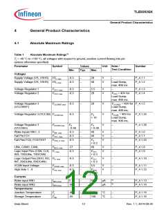
4
General Product Characteristics
4.1
Absolute Maximum Ratings
Table 1
Absolute Maximum Ratings1)
Tj = -40 °C to +150 °C; all voltages with respect to ground, positive current flowing into pin
(unless otherwise specified)
Parameter
Symbol
Values
Typ.
Unit Note /
Test Condition
Number
Min.
Max.
Voltages
Supply Voltage (VS, VSHS) VSx, max
Supply Voltage (VS, VSHS) VSx, max
-0.3
-0.3
–
–
28
40
V
V
–
P_4.1.1
P_4.1.2
Load Dump,
max. 400 ms
Voltage Regulator 1
Voltage Regulator 2
VCC1, max
VCC2, max
-0.3
-0.3
–
–
5.5
28
V
V
–
P_4.1.3
P_4.1.4
V
CC2 = 40V for
Load Dump,
max. 400 ms;
Voltage Regulator 3
(VCC3REF)
VCC3REF,max -0.3
–
–
–
28
V
V
V
VCC3REF = 40V for P_4.1.5
Load Dump,
max. 400 ms;
Voltage Regulator 3 (VCC3B) VCC3B,max
-0.3
VS
+ 10
V
CC3B = 40V for
P_4.1.25
P_4.1.26
Load Dump,
max. 400 ms;
Voltage Regulator 3
(VCC3SH)
VCC3SH,max VS
VS
+ 0.30
–
- 0.30
Wake Inputs WK1..3
Fail Pin FO1
VWK, max
VFO1, max
-0.3
–
–
–
40
40
V
V
V
–
–
–
P_4.1.6
P_4.1.7
P_4.1.23
-0.3
Fail Pins FO2, FO3/TEST
VFO2_3, max -0.3
VS
+ 0.3
LINx, CANH, CANL
VBUS, max
-27
–
–
40
V
V
–
–
P_4.1.8
P_4.1.9
Logic Input Pins (CSN, CLK, VI, max
-0.3
VCC1
SDI, TXDLINx, TXDCAN)
+ 0.3
Logic Output Pins (SDO, RO, VO, max
-0.3
–
VCC1
V
–
P_4.1.10
INT, RXDLINx, RXDCAN)
+ 0.3
VCAN Input Voltage
High Side 1...4
VVCAN, max
-0.3
-0.3
–
–
5.5
V
V
–
–
P_4.1.11
P_4.1.12
VHS, max
VSHS
+ 0.3
Currents
2)
2)
Wake input WK1
Wake input WK2
Temperatures
IWK1,max
IWK2,max
0
–
–
500
0
µA
µA
P_4.1.13
P_4.1.14
-500
Junction Temperature
Storage Temperature
Tj
-40
-55
–
–
150
150
°C
°C
–
–
P_4.1.15
P_4.1.16
Tstg
Data Sheet
12
Rev. 1.1, 2014-09-26

 INFINEON [ Infineon ]