PDF
最近搜索
热门搜索
发布采购

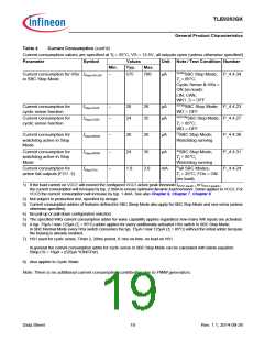
| 型号: | TLE9263QX |
| PDF下载: | 下载PDF文件 查看货源 |
| 内容描述: | [The device is designed for various CAN-LIN automotive applications as main supply for the microcontroller and as interface for a LIN and CAN bus network.] |
| 分类和应用: | |
| 文件页数/大小: | 164 页 / 6311 K |
| 品牌: |  INFINEON [ Infineon ] INFINEON [ Infineon ] |
专业IC领域供求交易平台:提供全面的IC Datasheet资料和资讯,Datasheet 1000万数据,IC品牌1000多家。