TLD7002-16ES
Datasheet
4 Power supply
4
Power supply
The device is supplied by VS, which is used for the internal logic and the supply for the power output stages.
Moreover, the high-speed lighting bus bias voltage VDD is generated internally from VS and available on the VDD pin.
VS has an undervoltage detection circuit, which prevents the activation of the power output stages and diagnosis in
case the applied voltage is below the undervoltage threshold.
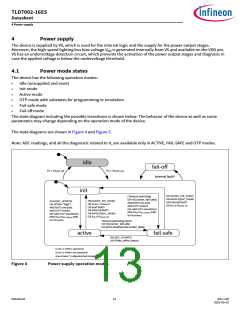
4.1
Power mode states
The device has the following operation modes:
•
•
•
•
•
•
Idle (unsupplied and reset)
Init mode
Active mode
OTP mode with substates for programming or emulation
Fail-safe mode
Fail-off mode
The state diagram including the possible transitions is shown below. The behavior of the device as well as some
parameters may change depending on the operation mode of the device.
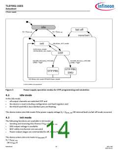
The state diagrams are shown in Figure 4 and Figure 5.
Note: ADC readings, and all the diagnostic related to it, are available only in ACTIVE, FAIL-SAFE and OTP modes.
idle
fail-off
VS < VS(UV)_fall
VS > VS(UV)_rise
2)
internal fault
init
HSLI(enter_init_mode)
OR 6xHSLI(sync_break)
(Timeout watchdog
OR HSLI(enter_fail-safe))
AND BISTs are pass
HSLI(enter_init_mode)
(HSLI(DC_UPDATE)
OR GPINn=“high“)
AND BISTs are pass
AND (OTP locked
OR valid OTP emulation)
AND (VDD>VDD_UV(rise) AND
1)
OR internal fault
3)
OR VERRN < VERRN,th
OR VDD ≤ VDD(UV)_fall
AND (OTP locked
3)
OR load fault
OR valid OTP emulation)
AND (VDD>VDD_UV(rise) AND
1)
OR internal fault
OR 6xHSLI(sync_break)
OR VDD ≤ VDD(UV)_fall
VS>VSOP(MIN)
)
VS>VSOP(MIN)
)
Timeout watchdog (WTD)
OR HSLI(enter_fail-safe)
OR (WTD disabled AND GPINn_WRN)
active
fail-safe
HSLI(DC_UPDATE)
OR GPINn_WRN cleared
1) HSLI or ERRN is operational
2) HSLI or ERRN is not operational
3) see chapter "Configurable fault management"
Figure 4
Power supply operation modes
Datasheet
13
Rev.1.00
2022-05-03

 INFINEON [ Infineon ]