TDA5235
Appendix
Register Description
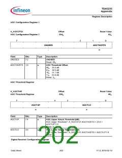
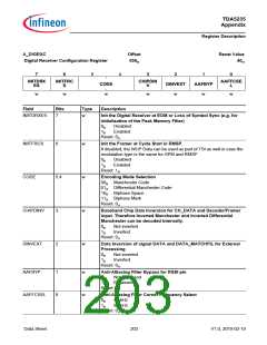
A_DIGRXC
Offset
036H
Reset Value
40H
Digital Receiver Configuration Register
ꢀ
ꢃ
ꢈ
ꢄ
ꢅ
ꢆ
',19(;7
Z
ꢇ
$$)%<3
Z
ꢁ
,1,7'5;
(6
,1,7)5&
6
&+,3',1
9
$$))&6(
/
&2'(
Z
Z
Z
Z
Z
Field
Bits
Type
Description
INITDRXES
7
w
Init the Digital Receiver at EOM or Loss of Symbol Sync (e.g. for
initialization of the Peak Memory Filter)
0B
1B
Disabled
Enabled
Reset: 0H
INITFRCS
6
w
Init the Framer at Cycle Start in RMSP.
If disabled, the WUP Data can be used as part of TSI as well in case the
modulation type is the same for SPM and RMSP
0B
1B
Disabled
Enabled
Reset: 1H
CODE
5:4
w
w
w
Encoding Mode Selection
00B Manchester Code
01B Differential Manchester Code
10B Biphase Space
11B Biphase Mark
Reset: 0H
CHIPDINV
DINVEXT
3
Baseband Chip Data Inversion for CH_DATA and Decoder/Framer
input. Therefore Inverted Manchester and Inverted Differential
Manchester can be decoded internally.
0B
1B
Not inverted
Inverted
Reset: 0H
2
Data Inversion of signal DATA and DATA_MATCHFIL for External
Processing
0B
1B
Not inverted
Inverted
Reset: 0H
AAFBYP
1
0
w
w
Anti-Alliasing Filter Bypass for RSSI pin
0B
1B
Not bypassed
Bypassed
Reset: 0H
AAFFCSEL
Anti-Alliasing Filter Corner Frequency Select
0B
1B
40 kHz
80 kHz
Reset: 0H
Data Sheet
203
V1.0, 2010-02-19

 INFINEON [ Infineon ]