TC1796
Functional Description
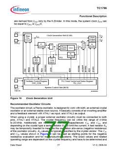
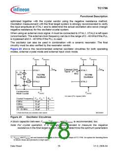
are derived from fVCO only by the K-Divider. In this mode, the system clock fSYS can
be equal to fCPU or fCPU/2.
XTAL1
fCPU
fSYS
Clock Generation Unit (CGU)
Main
Osc.
Circuit
fOSC
Clock
Output
Control
M
U
X
XTAL2
P-
Divider
K-
Divider
≥1
fP
fN
fVCO
Phase
Detect.
VCO
N-
Divider
PLL
PLL
Lock
Osc.
Run
Detect.
Detect.
BYPASS
Oscillator Control Register
OSC_CON
PLL Clock Control and Status Register
PLL_CLC
System Control Unit (SCU)
P5.3 /
TXD1A
MCB05600
Figure 19
Clock Generation Unit
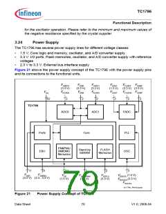
Recommended Oscillator Circuits
The oscillator circuit, a Pierce oscillator, is designed to work with both, an external crystal
oscillator or an external stable clock source. It basically consists of an inverting amplifier
and a feedback element with XTAL1 as input, and XTAL2 as output.
When using a crystal, a proper external oscillator circuitry must be connected to both
pins, XTAL1 and XTAL2. The crystal frequency can be within the range of 4 MHz
to 25 MHz. Additionally are necessary, two load capacitances CX1 and CX2, and
depending on the crystal type a series resistor RX2 to limit the current. A test resistor RQ
may be temporarily inserted to measure the oscillation allowance (negative resistance)
of the oscillator circuitry. RQ values are typically specified by the crystal vendor. The CX1
and CX2 values shown in Figure 20 can be used as starting points for the negative
resistance evaluation and for non-productive systems. The exact values and related
operating range are dependent on the crystal frequency and have to be determined and
Data Sheet
77
V1.0, 2008-04

 INFINEON [ Infineon ]