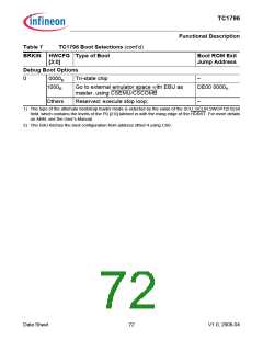
TC1796
Functional Description
3.23
Clock Generation and PLL
The TC1796 clock system performs the following functions:
•
Acquires and buffers incoming clock signals to create a master clock frequency
Distributes in-phase synchronized clock signals throughout the TC1796’s entire clock
tree
•
•
Divides a system master clock frequency into lower frequencies required by the
different modules for operation.
•
•
•
Dynamically reduces power consumption during operation of functional units
Statically reduces power consumption through programmable power-saving modes
Reduces electromagnetic interference (EMI) by switching off unused modules
The clock system must be operational before the TC1796 is able to run. Therefore, it also
contains special logic to handle power-up and reset operations. Its services are
fundamental to the operation of the entire system, so it contains special fail-safe logic.
Features
•
•
•
PLL operation for multiplying clock source by different factors
Direct drive capability for direct clocking
Comfortable state machine for secure switching between basic PLL, direct or
prescaler operation
•
Sleep and Power-Down Mode support
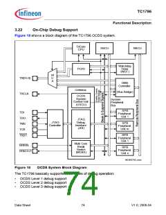
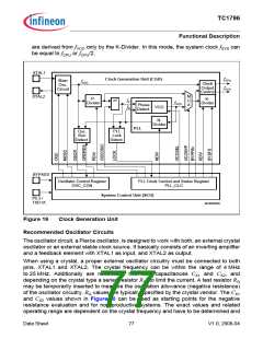
The TC1796 Clock Generation Unit (CGU) as shown in Figure 19 allows a very flexible
clock generation. It basically consists of an main oscillator circuit and a Phase- Locked
Loop (PLL). The PLL can converts a low-frequency external clock signal from the
oscillator circuit to a high-speed internal clock for maximum performance.
The system clock fSYS is generated from an oscillator clock fOSC in either of four
hardware/software selectable ways:
•
Direct Drive Mode (PLL Bypass):
In Direct Drive Mode, the PLL is bypassed and the CGU clock outputs are directly fed
from the clock signal fOSC, i.e. fCPU = fOSC and fSYS = fOSC/2 or fOSC. This allows
operation of the TC1796 with a reasonably small fundamental mode crystal.
VCO Bypass Mode (Prescaler Mode):
•
•
In VCO Bypass Mode, fCPU and fSYS are derived from fOSC by the two divider stages,
P-Divider and K-Divider. The system clock fSYS can be equal to fCPU or fCPU/2.
PLL Mode:
In PLL Mode, the PLL is running. The VCO clock fVCO is derived from fOSC, divided by
the P factor, multiplied by the PLL (N-Divider). The clock signals fCPU and fSYS are
derived from fVCO by the K-Divider. The system clock fSYS can be equal to fCPU or
f
CPU/2.
•
PLL Base Mode:
In PLL Base Mode, the PLL is running at its VCO base frequency and fCPU and fSYS
Data Sheet
76
V1.0, 2008-04

 INFINEON [ Infineon ]