TC1796
Functional Description
optimized together with the crystal vendor using the negative resistance method.
Oscillation measurement with the final target system is strongly recommended to verify
the input amplitude at XTAL1 and to determine the actual oscillation allowance (margin
negative resistance) for the oscillator-crystal system.
When using an external clock signal, it must be connected to XTAL1. XTAL2 is left open
(unconnected). The external clock frequency can be in the range of 0 - 40 MHz if the PLL
is bypassed and 4 - 40 MHz if the PLL is used.
The oscillator can also be used in combination with a ceramic resonator. The final
circuitry must be also verified by the resonator vendor.
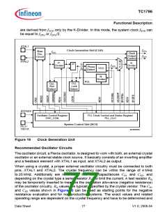
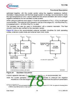
Figure 20 shows the recommended external oscillator circuitries for both operating
modes, external crystal mode and external input clock mode.
VDDOSC VDDOSC3
VDDOSC VDDOSC3
fOSC
fOSC
External Clock
Signal
XTAL1
XTAL1
41) - 40
MHz
4 - 25
MHz
TC1796
TC1796
Oscillator
Oscillator
RQ
RX2
CX2
XTAL2
XTAL2
CX1
Fundamental
Mode Crystal
VSSOSC
VSSOSC
1) in case of PLL bypass 0 MHz
1)
1)
CX1
,
CX2
RX2
Crystal Frequency
4 MHz
8 MHz
33 pF
18 pF
12 pF
10 pF
0
0
0
0
12 MHz
16 - 25 MHz
1) Note that these are evaluation start values!
MCS05601
Figure 20
Oscillator Circuitries
A block capacitor between VDDOSC1)/VDDOSC3 and VSSOSC is recommended, too.
Note: For crystal operation, it is strongly recommended to measure the negative
resistance in the final target system (layout) to determine the optimum parameters
1) VDDOSC and VSSOSC are not bonded externally in the BC and BD steps of TC1796. An option for bonding them
in future steps and products is kept open.
Data Sheet
78
V1.0, 2008-04

 INFINEON [ Infineon ]