TC1796
Functional Description
for the oscillator operation. Please refer to the minimum and maximum values of
the negative resistance specified by the crystal supplier.
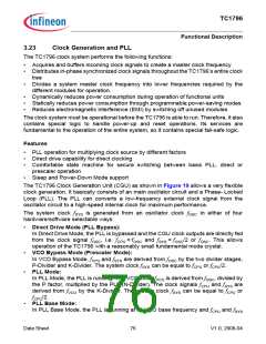
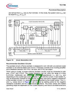
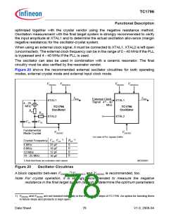
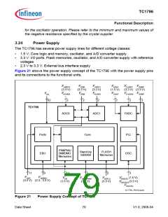
3.24
Power Supply
The TC1796 has several power supply lines for different voltage classes:
•
1.5 V: Core logic and memory, oscillator, and A/D converter supply
3.3 V: I/O ports, Flash memories, oscillator, and A/D converter supply with reference
voltages
•
•
2.3 V to 3.3 V: External bus interface supply
Figure 21 shows the power supply concept of the TC1796 with the power supply pins
and its connections to the functional units.
VAREF0
(3.3 V)
VAGND0
VDDM
(3.3 V)
VSSM
VAREF1
(3.3 V)
VAGND1
VDDAF
(1.5 V)
VSSAF
VFAREF VDDMF
(3.3 V) (3.3 V)
VFAGND VSSMF
VSS
62
2
2
2
2
2
2
TC1796
ADC0
ADC1
FADC
Ports
Core
PLL
PMI/PMU
DMI/DMU
Memories
Stand-by
SBRAM
FLASH
EBU
OSC
Memories
11
9
13
1
2
3
VDDP
VDDEBU
VDD
VDDSBRAM
VDDFL3
VDDOSC (1.5 V)
(3.3 V) (2.3 - 3.3 V)
(1.5 V)
(1.5 V)
(3.3 V)
V
DDOSC3 (3.3 V)
VSSOSC
tc1796_PwrSupply
Figure 21
Power Supply Concept of TC1796
Data Sheet
79
V1.0, 2008-04

 INFINEON [ Infineon ]