TC1796
General Device Information
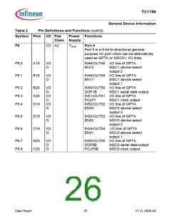
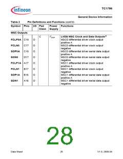
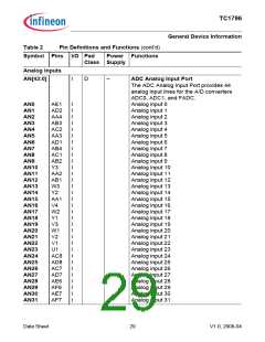
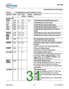
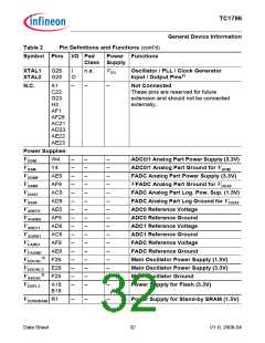
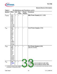
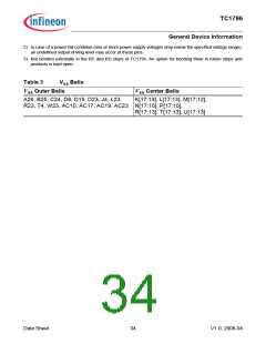
Table 2
Symbol Pins I/O Pad
Class Supply
Pin Definitions and Functions (cont’d)
Power Functions
D
–
ADC Analog Input Port (cont’d)
Analog input 32
AN32
AN33
AN34
AN35
AN36
AN37
AN38
AN39
AN40
AN41
AN42
AN43
AC3
AE2
AD3
AD5
AE3
AF2
AC4
AF3
AD4
AE4
AC5
AF4
I
I
I
I
I
I
I
I
I
I
I
I
Analog input 33
Analog input 34
Analog input 35
Analog input 36
Analog input 37
Analog input 38
Analog input 39
Analog input 40
Analog input 41
Analog input 42
Analog input 43
TR[15:0]
O
A3
VDDP
OCDS Level 2 Debug Trace Lines2)
(located on center balls)
Trace output line 0
Trace output line 1
Trace output line 2
Trace output line 3
Trace output line 4
Trace output line 5
Trace output line 4
Trace output line 7
Trace output line 8
Trace output line 9
Trace output line 10
Trace output line 11
Trace output line 12
Trace output line 13
Trace output line 14
Trace output line 15
TR0
U12
T12
U11
T11
U10
R12
R10
R11
M11
M10
L11
L10
K10
K11
L12
K12
O
O
O
O
O
O
O
O
O
O
O
O
O
O
O
O
TR1
TR2
TR3
TR4
TR5
TR6
TR7
TR8
TR9
TR10
TR11
TR12
TR13
TR14
TR15
TRCLK
T10
O
A4
Trace Clock for OCDS Level 2 Debug
Trace Lines1)
(located on a center ball)
Data Sheet
30
V1.0, 2008-04

 INFINEON [ Infineon ]