TC1796
General Device Information
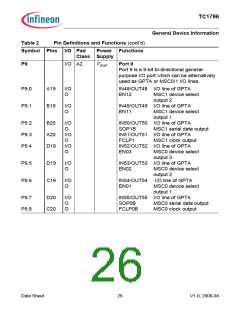
Table 2
Symbol Pins I/O Pad
Class Supply
A1
Pin Definitions and Functions (cont’d)
Power Functions
P10
I
VDDP
Hardware Configuration Inputs / Port 10
These inputs are boot mode (hardware
configuration) control inputs. They are
latched with the rising edge of HDRST.
Port 10 input line 0 / HWCFG0
P10.0
P10.1
P10.2
P10.3
A21
B21
C21
D21
I
I
I
I
Port 10 input line 1 / HWCFG1
Port 10 input line 2 / HWCFG2
Port 10 input line 3 / HWCFG3
After reset (HDRST = 1) the state of the
Port 10 input pins may be modified from the
reset configuration state. There actual state
can be read via software (P10_IN register).
During normal operation input HWCFG1
serves as emergency shut-off control input
for certain I/O lines (e.g. GPTA related
outputs).
Dedicated Peripheral I/Os
SLSO0
SLSO1
MTSR0
AE14 O
AC15 O
AF15 O
I
A2
VDDP
SSC0 Slave Select Output Line 0
SSC0 Slave Select Output Line 1
SSC0 Master Transmit Output /
SSC0 Slave Receive Input
MRST0
AE15 I
O
SSC0 Master Receive Input /
SSC0 Slave Transmit Output
SCLK0
SLSI0
AF14 I/O
AD15 I
SSC0 Clock Input/Output
SSC0 Slave Select Input
Data Sheet
27
V1.0, 2008-04

 INFINEON [ Infineon ]