TC1796
General Device Information
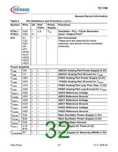
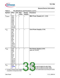
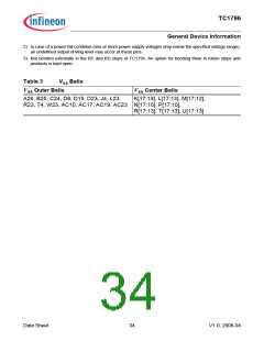
Table 2
Symbol Pins I/O Pad
Class Supply
Pin Definitions and Functions (cont’d)
Power Functions
XTAL1
G26
G25
I
O
n.a.
VDD
Oscillator / PLL / Clock Generator
XTAL2
Input / Output Pins2)
N.C.
A1
–
–
–
Not Connected
C22
These pins are reserved for future
extension and should not be connected
externally.
G23
H3
AF1
AF26
AC21
AD23
AE22
AE23
Power Supplies
VDDM
VSSM
W4
Y4
–
–
–
–
–
–
–
–
–
–
–
–
–
–
–
–
–
–
–
–
–
–
–
–
–
–
–
–
–
–
–
–
–
–
–
–
–
–
–
–
–
–
–
–
–
–
–
–
ADC0/1 Analog Part Power Supply (3.3V)
ADC0/1 Analog Part Ground for VDDM
FADC Analog Part Power Supply (3.3V)
VFADC Analog Part Ground for VDDAF
FADC Analog Part Log. Pow. Sup. (1.5V)
FADC Analog Part Log Ground for VDDAF
ADC0 Reference Voltage
ADC0 Reference Ground
ADC1 Reference Voltage
ADC1 Reference Ground
FADC Reference Voltage
VDDMF
VSSMF
VDDAF
VSSAF
VAREF0
VAGND0
VAREF1
VAGND1
VFAREF
VFAGND
VDDOSC
AE9
AF9
AC9
AD9
AE5
AF5
AD6
AC6
AF8
AE8
F26
FADC Reference Ground
3)
Main Oscillator Power Supply (1.5V)
Main Oscillator Power Supply (3.3V)
Main Oscillator Ground
VDDOSC3 E26
VSSOSC
VDDFL3
3)
F25
A18
B18
Power Supply for Flash (3.3V)
VDDSBRAM R1
–
–
–
Power Supply for Stand-by SRAM (1.5V)
Data Sheet
32
V1.0, 2008-04

 INFINEON [ Infineon ]