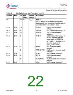
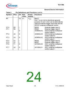
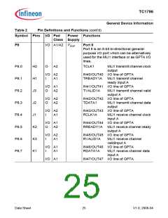
TC1796
General Device Information
Table 2
Symbol Pins I/O Pad
Class Supply
I/O A2
Pin Definitions and Functions (cont’d)
Power Functions
P9
VDDP
Port 9
Port 9 is a 9-bit bi-directional general-
purpose I/O port which can be alternatively
used as GPTA or MSC0/1 I/O lines.
P9.0
P9.1
A19
B19
I/O
O
IN48/OUT48 I/O line of GPTA
EN12
MSC1 device select
output 2
I/O
O
IN49/OUT49 I/O line of GPTA
EN11
MSC1 device select
output 1
P9.2
P9.3
P9.4
B20
A20
D18
I/O
O
IN50/OUT50 I/O line of GPTA
SOP1B
MSC1 serial data output
I/O
O
IN51/OUT51 I/O line of GPTA
FCLP1
MSC1 clock output
I/O
O
IN52/OUT52 I/O line of GPTA
EN03
MSC0 device select
output 3
P9.5
P9.6
D19
C19
I/O
O
IN53/OUT53 I/O line of GPTA
EN02
MSC0 device select
output 2
I/O
O
IN54/OUT54 I/O line of GPTA
EN01
MSC0 device select
output 1
P9.7
P9.8
D20
C20
I/O
O
O
IN55/OUT55 I/O line of GPTA
SOP0B
FCLP0B
MSC0 serial data output
MSC0 clock output
Data Sheet
26
V1.0, 2008-04

 INFINEON [ Infineon ]