TC1796
General Device Information
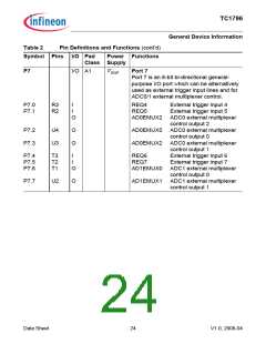
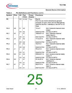
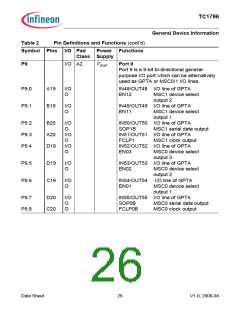
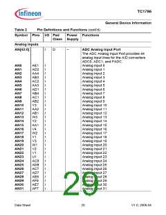
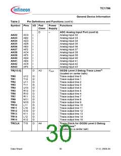
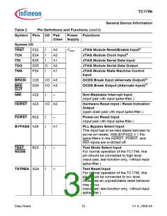
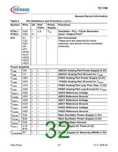
Table 2
Symbol Pins I/O Pad
Class Supply
Pin Definitions and Functions (cont’d)
Power Functions
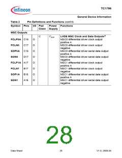
MSC Outputs
C
VDDP
LVDS MSC Clock and Data Outputs2)
MSC0 differential driver clock output
positive A
FCLP0A C18
O
O
O
O
O
O
O
O
FCLN0
SOP0A
SON0
C17
C16
D17
MSC0 differential driver clock output
negative
MSC0 differential driver serial data output
positive A
MSC0 differential driver serial data output
negative
FCLP1A A17
MSC1 differential driver clock output
positive A
FCLN1
SOP1A
SON1
B17
B16
A16
MSC1 differential driver clock output
negative
MSC1 differential driver serial data output
positive A
MSC1 differential driver serial data output
negative
Data Sheet
28
V1.0, 2008-04

 INFINEON [ Infineon ]