TC1796
General Device Information
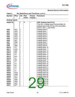
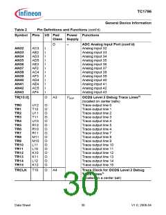
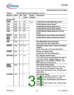
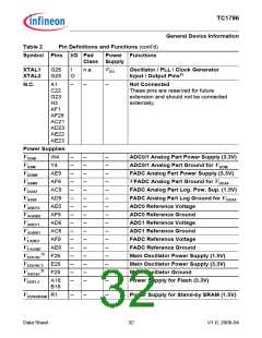
Table 2
Symbol Pins I/O Pad
Class Supply
Pin Definitions and Functions (cont’d)
Power Functions
VDDEBU
H23
H24
H25
H26
M23
T23
–
–
–
EBU Power Supply (2.3 - 3.3V)
Y23
AC18
AC22
VDD
B26
C25
D9
–
–
–
Core Power Supply (1.5V)
D16
D24
E23
H4
P23
R4
V23
AB23
AC11
AC20
VDDP
A25
B24
C23
D7
D14
D22
K4
–
–
–
Port Power Supply (3.3V)
(also for OCDS)
AC16
AD16
AE16
AF16
VSS
See
Table
3
–
–
–
Ground
15 VSS lines are located at outer balls.
47 VSS lines are located at center balls.
1) In order to minimize noise coupling to the on-chip A/D converters, it is recommended to use these pins as less
as possible in strong driver mode.
Data Sheet
33
V1.0, 2008-04

 INFINEON [ Infineon ]