TC1796
General Device Information
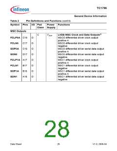
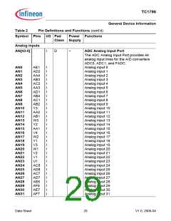
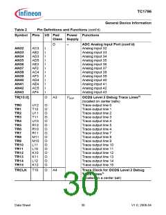
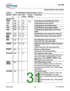
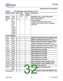
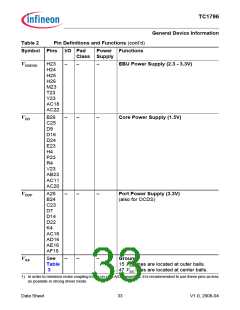
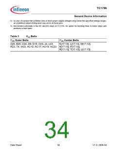
Table 2
Symbol Pins I/O Pad
Class Supply
Pin Definitions and Functions (cont’d)
Power Functions
System I/O
TRST
TCK
TDI
TDO
TMS
F23
I
I
I
O
I
A2
A2
A1
A2
A1
VDDP
JTAG Module Reset/Enable Input2)
JTAG Module Clock Input2)
JTAG Module Serial Data Input
JTAG Module Serial Data Output
E24
E25
D25
F24
JTAG Module State Machine Control
Input
BRKIN
C26
D26
I/O A3
I/O A3
OCDS Break Input (Alternate Output)2)
OCDS Break Output (Alternate Input)2)
BRK
OUT
NMI
A22
I
–
Non-Maskable Interrupt Input
(input pad with input spike-filter.)
HDRST A23
I/O A2
Hardware Reset Input / Reset Indication
Output
(open drain pad with input spike-filter.)
PORST B22
BYPASS A24
I
I
–
Power-on Reset Input
(input pad with input spike-filter.)
A1
PLL Bypass Select Input
This input has to be held stable between to
power-on resets. With BYPASS = 1 the
spike filters in the HDRST, PORST, and
NMI inputs are switched off.
TEST
B23
I
I
–
–
Test Mode Select Input
MODE
For normal operation of the TC1796, this
pin should be connected to high level.
(input pad, test function only, without input
spike-filter.)
TSTRES G24
Test Reset Input
For normal operation of the TC1796, this
pin should be connected to low level.
Otherwise an unpredictable reset behavior
may occur.
(input pad, test function only, without input
spike-filter.)
Data Sheet
31
V1.0, 2008-04

 INFINEON [ Infineon ]