TC1796
Electrical Parameters
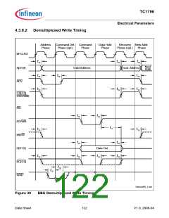
4.3.12
Peripheral Timings
Note: Peripheral timing parameters are not subject to production test. They are verified
by design/characterization.
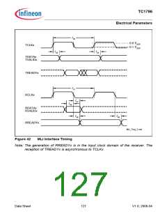
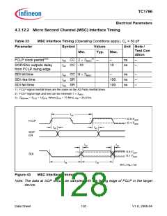
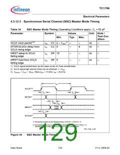
4.3.12.1 Micro Link Interface (MLI) Timing
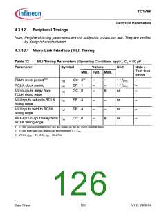
Table 32
MLI Timing Parameters (Operating Conditions apply), CL = 50 pF
Parameter
Symbol
Values
Min. Typ. Max.
Unit
Note /
Test Con
dition
TCLK clock period1)2)
RCLK clock period
MLI outputs delay from
TCLK rising edge
t30
t31
t35
CC 23)
SR 1
CC 0
–
–
–
–
–
8
1 / fSYS
1 / fSYS
ns
–
–
–
MLI inputs setup to RCLK
falling edge
MLI inputs hold to RCLK
falling edge
t36
t37
SR 4
SR 4
CC 0
–
–
–
–
–
8
ns
ns
ns
–
–
–
RREADY output delay from t38
RCLK falling edge
1) TCLK signal rise/fall times are the same as the A2 Pads rise/fall times.
2) TCLK high and low times can be minimum 1 × TMLI.
3) When fSYS = 75 MHz, t30 = 26,67ns
Data Sheet
126
V1.0, 2008-04

 INFINEON [ Infineon ]