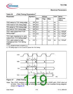
TC1796
Electrical Parameters
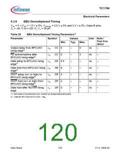
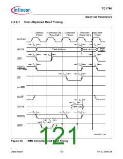
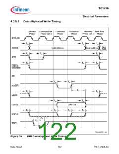
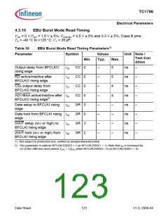
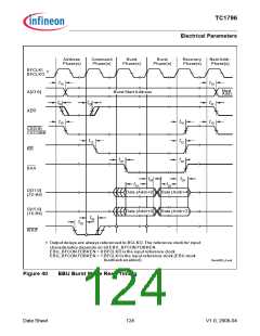
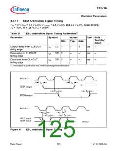
4.3.10
EBU Burst Mode Read Timing
VSS = 0 V;VDD = 1.5 V ± 5%; VDDEBU = 2.5 V ± 5% and 3.3 V ± 5%, Class B pins;
TA = -40 °C to +125 °C; CL = 35 pF;
Table 30
EBU Burst Mode Read Timing Parameters1)
Parameter
Symbol
Values
Typ.
Unit Note /
Test Con
Min.
Max.
dition
Output delay from BFCLKO
rising edge
RD active/inactive after
BFCLKO rising edge
CSx output delay from
BFCLKO rising edge
t10
t12
t21
CC 0
–
–
–
–
–
–
–
–
5
ns
ns
ns
ns
ns
ns
ns
ns
–
CC 0
5
4
4
–
–
–
–
–
–
–
–
–
–
–
CC 0
CC 0
SR 3
SR 0
SR 3
SR 2
ADV/BAA active/inactive after t22
BFCLKO rising edge2)
Data setup to BFCLKI rising
edge
t23
Data hold from BFCLKI rising t24
edge
WAIT setup (low or high) to
BFCLKI rising edge
t25
WAIT hold (low or high) from t26
BFCLKI rising edge
1) Not subject to production test, verified by design/characterization.
2) This parameter is valid for BFCON.EBSE0 = 1 (or BFCON.EBSE1 = 1). Note that t22 is increased by:
1/2 of the LMB bus clock period TCPU = 1/fCPU when BFCON.EBSE0 = 0 (or BFCON.EBSE1 = 0).
Data Sheet
123
V1.0, 2008-04

 INFINEON [ Infineon ]