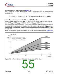
C167CR
C167SR
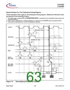
8)
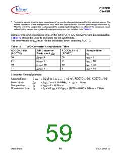
During the sample time the input capacitance CAIN can be charged/discharged by the external source. The
internal resistance of the analog source must allow the capacitance to reach its final voltage level within tS.
After the end of the sample time tS, changes of the analog input voltage have no effect on the conversion result.
Values for the sample time tS depend on programming and can be taken from Table 13.
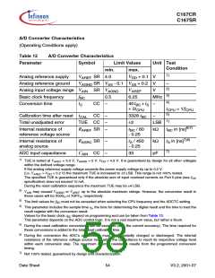
Sample time and conversion time of the C167CR’s A/D Converter are programmable.
Table 13 should be used to calculate the above timings.
The limit values for fBC must not be exceeded when selecting ADCTC.
Table 13
A/D Converter Computation Table
ADCON.15|14
(ADCTC)
A/D Converter
Basic clock fBC
ADCON.13|12
(ADSTC)
Sample time
tS
00
01
10
11
f
f
f
f
CPU / 4
CPU / 2
CPU / 16
CPU / 8
00
01
10
11
tBC × 8
tBC × 16
tBC × 32
tBC × 64
Converter Timing Example:
Assumptions:
fCPU = 25 MHz (i.e. tCPU = 40 ns), ADCTC = ‘00’, ADSTC = ‘00’.
Basic clock
Sample time
Conversion time tC
fBC
tS
= fCPU / 4 = 6.25 MHz, i.e. tBC = 160 ns.
= tBC × 8 = 1280 ns.
= tS + 40 tBC + 2 tCPU = (1280 + 6400 + 80) ns = 7.8 µs.
Data Sheet
55
V3.2, 2001-07

 INFINEON [ Infineon ]