C167CR
C167SR
AC Characteristics
Table 14
CLKOUT Reference Signal
Parameter
Symbol
Limits
min. max.
Unit
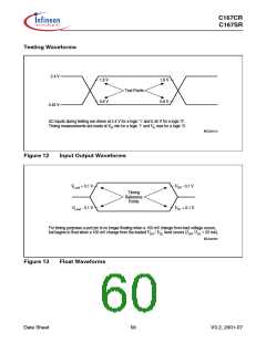
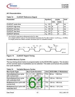
CLKOUT cycle time
CLKOUT high time
CLKOUT low time
CLKOUT rise time
CLKOUT fall time
tc5 CC
301)
ns
ns
ns
ns
ns
tc6 CC 8
tc7 CC 6
tc8 CC –
tc9 CC –
–
–
4
4
1)
The CLKOUT cycle time is influenced by the PLL jitter.
For a single CLKOUT cycle (2 TCL) the deviation caused by the PLL jitter is below 1 ns (for fCPU > 25 MHz).
For longer periods the relative deviation decreases (see PLL deviation formula).
tc9
tc7
tc8
tc5
tc6
CLKOUT
MCT04415
Figure 14
CLKOUT Signal Timing
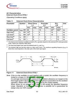
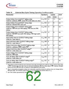
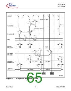
Variable Memory Cycles
The bus timing shown below is programmable via the BUSCONx registers. The duration
of ALE and two types of waitstates can be selected. This table summarizes the possible
bus cycle durations.
Table 15
Variable Memory Cycles
Bus Cycle Type
Bus Cycle Duration
Unit 25/33 MHz, 0 Waitstates
Demultiplexed bus cycle
with normal ALE
4 + 2 × (15 - <MCTC>) TCL 80 ns / 60.6 ns
+ 2 × (1 - <MTTC>)
Demultiplexed bus cycle
with extended ALE
6 + 2 × (15 - <MCTC>) TCL 120 ns / 90.9 ns
+ 2 × (1 - <MTTC>)
Multiplexed bus cycle with 6 + 2 × (15 - <MCTC>) TCL 120 ns / 90.9 ns
normal ALE + 2 × (1 - <MTTC>)
Multiplexed bus cycle with 8 + 2 × (15 - <MCTC>) TCL 160 ns / 121.2 ns
extended ALE
+ 2 × (1 - <MTTC>)
Data Sheet
57
V3.2, 2001-07

 INFINEON [ Infineon ]