C167CR
C167SR
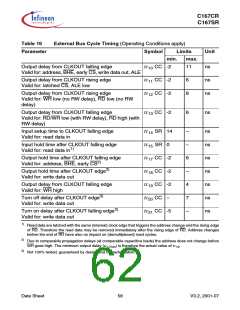
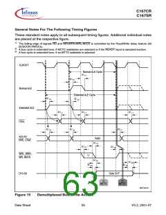
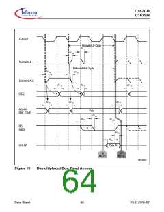
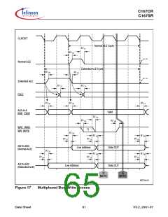
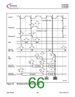
General Notes For The Following Timing Figures
These standard notes apply to all subsequent timing figures. Additional individual notes
are placed at the respective figure.
1)
The falling edge of signals RD and WR/WRH/WRL/WrCS is controlled by the Read/Write delay feature (bit
BUSCON.RWDCx).
2)
A bus cycle is extended here, if MCTC waitstates are selected or if the READY input is sampled inactive.
A bus cycle is extended here, if an MTTC waitstate is selected.
3)
CLKOUT
Normal ALE Cycle
tc11
tc10
Normal ALE
Extended ALE Cycle
tc10
tc10
Extended ALE
CSxL
tc11
tc11
tc11
tc10
tc10
tc17
A23-A0
BHE, CSxE
Valid
tc13
tc12
tc19
WRL, WRH,
WR, WrCS
1)
tc10
tc20
tc21
tc18
D15-D0
Data OUT
2)
MCTC
3)
MTTC
MCT04416
Figure 15
Demultiplexed Bus, Write Access
Data Sheet
59
V3.2, 2001-07

 INFINEON [ Infineon ]