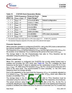
C167CR
C167SR
A/D Converter Characteristics
(Operating Conditions apply)
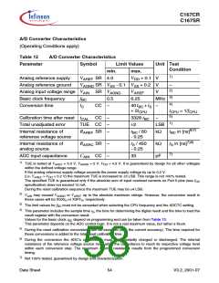
Table 12
A/D Converter Characteristics
Parameter
Symbol
Limit Values
min. max.
Unit Test
Condition
1)
Analog reference supply
Analog reference ground
VAREF SR 4.0
V
DD + 0.1 V
VAGND SR VSS - 0.1 VSS + 0.2 V
–
2)
Analog input voltage range VAIN SR VAGND
VAREF
V
3)
4)
Basic clock frequency
Conversion time
fBC
tC
0.5
CC –
6.25
MHz
–
40tBC +tS
+ 2tCPU
t
CPU = 1/fCPU
5)
Calibration time after reset tCAL CC –
3328 tBC
–
1)
Total unadjusted error
TUE CC –
RAREF SR –
2
LSB
kΩ
Internal resistance of
reference voltage source
t
BC / 60
- 0.25
t
BC in [ns]6)7)
Internal resistance of
analog source
RASRC SR –
CAIN CC –
tS / 450
- 0.25
kΩ
tS in [ns]7)8)
7)
ADC input capacitance
33
pF
1)
TUE is tested at VAREF = 5.0 V, VAGND = 0 V, VDD = 4.9 V. It is guaranteed by design for all other voltages
within the defined voltage range.
If the analog reference supply voltage exceeds the power supply voltage by up to 0.2 V
(i.e. VAREF = VDD + 0.2 V) the maximum TUE is increased to 3 LSB. This range is not 100% tested.
The specified TUE is guaranteed only if the absolute sum of input overload currents on Port 5 pins (see IOV
specification) does not exceed 10 mA.
During the reset calibration sequence the maximum TUE may be 4 LSB.
2)
VAIN may exceed VAGND or VAREF up to the absolute maximum ratings. However, the conversion result in
these cases will be X000 or X3FF , respectively.
H
H
3)
4)
The limit values for fBC must not be exceeded when selecting the CPU frequency and the ADCTC setting.
This parameter includes the sample time tS, the time for determining the digital result and the time to load the
result register with the conversion result.
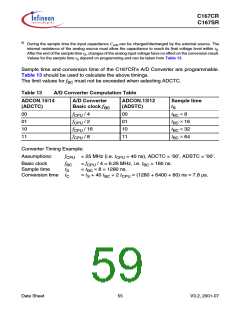
Values for the basic clock tBC depend on programming and can be taken from Table 13.
This parameter depends on the ADC control logic. It is not a real maximum value, but rather a fixum.
5)
6)
During the reset calibration conversions can be executed (with the current accuracy). The time required for
these conversions is added to the total reset calibration time.
During the conversion the ADC’s capacitance must be repeatedly charged or discharged. The internal
resistance of the reference voltage source must allow the capacitance to reach its respective voltage level
within each conversion step. The maximum internal resistance results from the programmed conversion
timing.
7)
Not 100% tested, guaranteed by design and characterization.
Data Sheet
54
V3.2, 2001-07

 INFINEON [ Infineon ]