C167CR
C167SR
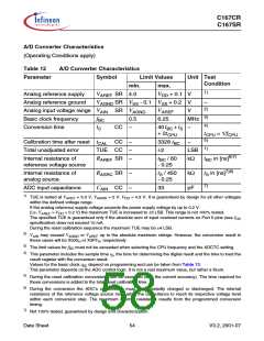
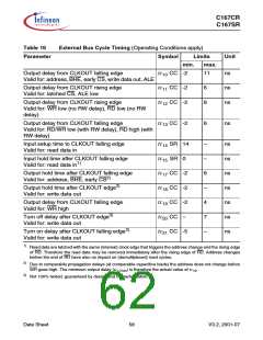
Table 16
External Bus Cycle Timing (Operating Conditions apply)
Symbol Limits
Parameter
Unit
min.
max.
Output delay from CLKOUT falling edge
Valid for: address, BHE, early CS, write data out, ALE
tc10 CC -2
tc11 CC -2
tc12 CC -2
11
ns
ns
ns
Output delay from CLKOUT rising edge
Valid for: latched CS, ALE low
6
8
Output delay from CLKOUT rising edge
Valid for: WR low (no RW delay), RD low (no RW
delay)
Output delay from CLKOUT falling edge
Valid for: RD/WR low (with RW delay), RD high (with
RW delay)
tc13 CC -2
6
ns
Input setup time to CLKOUT falling edge
Valid for: read data in
tc14 SR 14
tc15 SR 0
tc17 CC -2
tc18 CC -2
tc19 CC -2
tc20 CC –
tc21 CC -5
–
–
6
–
4
7
–
ns
ns
ns
ns
ns
ns
ns
Input hold time after CLKOUT falling edge
Valid for: read data in1)
Output hold time after CLKOUT falling edge
Valid for: address, BHE, early CS2)
Output hold time after CLKOUT edge3)
Valid for: write data out
Output delay from CLKOUT falling edge
Valid for: WR high
Turn off delay after CLKOUT edge3)
Valid for: write data out
Turn on delay after CLKOUT falling edge3)
Valid for: write data out
1)
Read data are latched with the same (internal) clock edge that triggers the address change and the rising edge
of RD. Therefore the read data may be removed immediately after the rising edge of RD. Address changes
before the end of RD have also no impact on (demultiplexed) read cycles.
2)
3)
Due to comparable propagation delays (at comparable capacitive loads) the address does not change before
WR goes high. The minimum output delay (tc17min) is therefore the actual value of tc19.
Not 100% tested, guaranteed by design and characterization.
Data Sheet
58
V3.2, 2001-07

 INFINEON [ Infineon ]