SAE 81C90/91
07Feb95@09:05h Intermediate Version
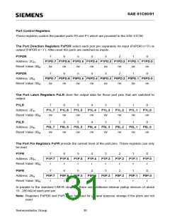
Host Interfaces
There are two different host interfaces implemented in the SAE 81C90/91.
Data and addresses on a multiplexed 8-bit bus, compatible with Siemens microcontrollers
(C5xx, C16x), can be transferred via the parallel interface (PI). Using the serial synchronous
interface (Sl), any host controller with a serial three-lead interface can be connected with.
The interface is selected by hardware through the wiring of the MS (Mode Select) pin. This pin may
not be switched during operation. If there is a High level on the MS pin, the SI and thus pins DI, DO,
CLK, W and TIM are activated, while pins AD5 through AD7, RD, WR and ALE are inactive. A Low
level on the MS pin switches to the Pl and thus activates pins AD0 through AD7, RD, WR and ALE.
Parallel Interface Pl
The parallel interface uses a multiplexed 8-bit address/data bus. First the address of the required
register is applied to the pins AD0 through AD7. A falling edge on pin ALE means that this address
is transferred to an on-chip latch. After this, data can either be written into the selected register (pin
WR = 0) or read from it (pin RD = 0) via the address/data bus. Pin CS must be 0 for the entire
duration of the RD/WR active time so that the circuit is activated.
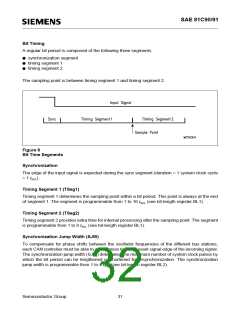
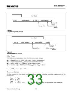
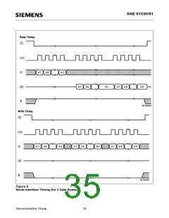
Serial Synchronous Interface Sl
If the SI is used the unused pins of PI must be set to inactive levels (RD, WR to VDD and ALE, AD5,
AD6, AD7 to VSS).
Communication on the SI is accomplished according to the following procedure:
Each access to the stand-alone Full-CAN circuit has to be started by activating the device (CS = 0).
After the beginning of access, an address must be written first and then data can be read or written.
The required function is determined by pin W (W = 1: read; W = 0: write). If the automatic
decrementing of the address is activated (bit ADE in the MOD register), any number of data bytes
can be accessed in succession. Finally the device has to be deactivated.
Procedure:
● Activate device (CS = 0)
● Set pin W to 1 for read, to 0 for write
● Write in address of first data byte
● Read out/write in one or more data bytes
● Deactivate device (CS = 1)
The most-significant bit is always output as the first bit of an address or a data byte.
Data from pin DI are transferred into the internal shift register with the rising edge of the clock. The
active clock edge of pin DO is selectable via the pin TIM. If this pin is 0 the data are output from the
shift register to pin DO with the rising clock edge (Timing A). If the pin TIM is 1, the output of data
is done with the falling edge (Timing B).
The timing for reading and writing of two data bytes with automatic decrementing activated is
illustrated below.
Semiconductor Group
33

 INFINEON [ Infineon ]